Electronic Technology Forum
Method of CMOS Operational Amplifier to Improve Power Supply Rejection Ratio
CMOS improves power supply rejection ratio
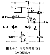
The reason why the power supply rejection ratio of the op amp circuit shown in Figure 3.6-1 is relatively poor is mainly caused by the coupling of the signal of the power supply change to the output terminal through the compensation capacitor. If some improvements are made to the op amp circuit in Figure 3.6-1 and its input is changed to a cascode form, the performance of its power supply rejection ratio will be improved. The specific circuit form is shown in Figure 3.6-2. When the power supply VDD has a change signal Vs, the output tube the gate also has the same changing signal. After the common gate circuit image.png is introduced, the signal from the drain has little effect on the source, so the signal coupled to the output terminal through the compensation capacitor Cc is also greatly reduced, thereby improving the power supply rejection ratio.
The disadvantage of the circuit in Figure 3.6-2 is that the input common-mode voltage is reduced, and its improved form is shown in Figure 3.6-3. This circuit has high common-mode input voltage and high power supply rejection ratio.

The first stage of this CMOS op amp circuit is basically the same as the high-speed CMOS op amp cascode circuit introduced in the previous section. The second stage is composed of M8 and M9 as the common source amplifier output circuit, due to the compensation capacitor One end of Cc is a common gate circuit therefore, the power supply rejection ratio performance is improved. From the equivalent circuit analysis (see Reference [21]), the power supply rejection ratio of this circuit is

where is the transconductance of the input pair M1 and M2,
 Is the transconductance of the
  tube,
tube, for
for
 equivalent output impedance,
 for
for equivalent output impedance,
 Is the transconductance of the output stage
  , C2 is
 the gate-source capacitance of the tube, Cc is the compensation capacitance.
and

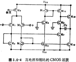
The circuit shown in Figure 3.6-4 has high power supply rejection ratio performance. The compensation capacitor Cc of this CMOS operational amplifier is also connected to the common gate circuit. the source of the tube. The input stage of the circuit is a current conversion type circuit, which is different from the usual op amp in that it adds a common gate circuit
 ,therefore, the power supply rejection ratio is improved.

Contact: Mr. Zou
Contact number: 0755-83888366-8022
Mobile phone: 18123972950
QQ: 2880195519
Contact Address: 5C1, Block CD, Tianji Building, Tianan Digital City, Chegongmiao, Futian District, Shenzhen
Please search WeChat official account: "KIA Semiconductor" or scan the following picture to "Follow" official WeChat official account
Please "follow" the official WeChat account: provide MOS tube technical assistance


