Electronic Technology Forum
Analyze the design of low voltage CMOS operational amplifier and current conversion type low power consumption
1. Design of low-voltage, low-power CMOS operational amplifier
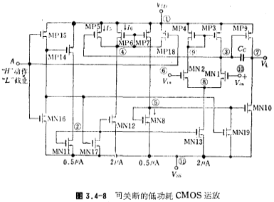
The design of low-voltage, low-power CMOS op amp is not difficult. It is not much different from general CMOS op amps. Here is a current-turn-off, low-power CMOS op amp circuit. Its circuit structure and parameters are shown in the figure. As shown in 3.4-8, the power supply voltage of this circuit is ±1.5 volts, and the quiescent current is about 9 microamperes, so the power consumption is only 27 microwatts. It is a two-stage amplifying circuit, the input stage is a differential amplifier composed of MN1, MN2, MP3 and MP4, and the second stage is a common source amplifier composed of MP9 and MN10; in order to increase the negative output capability of the output stage, MP6~MP7 are added When the voltage at the output terminal ③ of the differential amplifier increases, the voltage at the output terminal becomes negative. At the same time, MP5 current decreases, MP6, MP7, current increases, node ⑥ voltage increases, and MN10 current increases. Thereby enhancing the negative output capability. Low-voltage, low-power CMOS operational amplifier. Conversely, when the voltage of node ③ decreases, the output voltage increases. At the same time, the voltage of node ⑥ decreases, and the current of MN10 decreases, which increases the forward output capability. Therefore, the output stage circuit is actually push-pull.

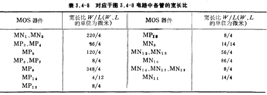
Type amplifier, so it has strong positive and negative drive capability, and low static power consumption. MP1s5, MP16, MN18, MN17, and MN10 in the circuit constitute a current control circuit. When point A is connected to a low potential (Vss), MP15 and MP16 are turned on, and MN16 is turned off. Because MP16 is turned on, the bias circuit MP14 and MN11 currents are zero, and MN17 and MN16 are turned on, so that MN12, MN11, and MN10 are turned on. Deadline. Because MP10 is turned on, MP6~MP7 are also turned off. In this way, the circuit is in an off state. When point A is connected to a high potential (VDD), the circuit is in a normal working state. At this time, the current control circuits MP15, MP16, MN17, and MN18 are in an off state, and MN18 is in an on state. Low-voltage, low-power CMOS operational amplifier. The open-loop gain of this circuit is greater than 1000. The width-to-length ratio of the circuit in Figure 3.4-8 is listed in Table 3.4-8.

2. Current conversion type low power CMOS operational amplifier
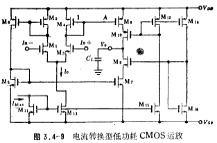
Here we introduce a current conversion type low-power CMOS operational amplifier, the circuit is shown in Figure 3.4-9. It is a typical current conversion type operational amplifier, which converts the input voltage into current, which is amplified by the current source circuit and sent to the output.

The working principle of the circuit in Figure 3.4-9 is now explained. It is a current conversion type low-power CMOS operational amplifier, M1~M4 are differential amplifiers, which convert the input signal voltage into current;
It is a current source circuit, which amplifies the current of the input stage and sends it to the output stage; M7~M9 are output stage circuits, which convert the output current into a voltage output; M12, M14, M15 and M16 provide output tubes M9, M10 The DC bias voltage of the grid; M11 is the bias circuit. Under static conditions, the currents of M6 and M7 are the same, so that the output voltage is zero. When the positive input signal acts on the gate of M1 (the gate of M3 is grounded), the current of M1 tube increases, the current of M3 tube decreases, the current through the current source circuit M7 increases, and the current M8 decreases, so that at the output end Obtain a negative direction proportional to the difference between the currents of the M7 and M8 two tubes
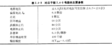
Output voltage, when a negative input signal is applied to the gate of M1 ( the grid is grounded), and the positive output voltage proportional to the difference between the currents of the M8 and M7 diodes is obtained at the output. Low-voltage, low-power CMOS operational amplifier. In order to obtain a higher voltage gain, the output stage (M7~M10) adopts a common-deep common-gate circuit to increase the output impedance, but the output dynamic amplitude is reduced. The main parameters of this circuit are listed in Table 3.4-9. Figure 3.4-9 The width-to-length ratio of the circuit tube is listed in Table 3.4-10.


Contact: Mr. Zou
Contact number: 0755-83888366-8022
Mobile phone: 18123972950
QQ: 2880195519
Contact Address: 5C1, Block CD, Tianji Building, Tianan Digital City, Chegongmiao, Futian District, Shenzhen
Please search WeChat official account: "KIA Semiconductor" or scan the following picture to "Follow" official WeChat official account
Please "follow" the official WeChat account: provide MOS tube technical assistance


