Electronic Technology Forum
CMOS operational amplifier power supply rejection ratio (PSRR) details and analysis
The power supply rejection ratio (PSRR) is defined as the ratio of the output voltage change corresponding to the power supply voltage change converted to the value of the input terminal, namely

In the formula, A is the open loop gain of the operational amplifier, Vs is the power supply voltage, and Vo is the output voltage.
In recent years, MOS large-scale integrated circuits have both analog and digital circuits, that is, the analog circuit and the digital circuit are built on the same chip, so the pulse signal of the digital circuit often interferes with the analog circuit (such as the operational amplifier circuit) through the power supply. , This interference signal causes the op amp to produce an output signal without signal input, thereby affecting the normal operation of the op amp circuit. In the monolithic operational amplifier circuit, this kind of power interference can be eliminated by using methods such as decoupling or separation from the power supply of the digital circuit. CMOS op amp power supply rejection ratio. But in MOS large-scale integrated circuits, this kind of interference often exists objectively and is difficult to eliminate. Therefore, in MOS large-scale integrated circuits, it is very necessary to design an operational amplifier with a high power supply rejection ratio.
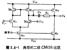
The circuit shown in Figure 3.6-1 is a typical two-level CMOS op amp, and its positive power supply suppression is relatively poor. CMOS op amp power supply rejection ratio. When there is an alternating signal voltage Vs on the positive power supply VDD, in order to keep the current of the output drive tube M6 constant (because the current of the M7 tube is constant), there is also a signal voltage Vs at the gate of M6, that is, The drain voltage increment of M6 is the same as the gate increment of M6, and the gate of M6 is connected to the compensation capacitor Cc. Therefore, the change signal of the M6 gate is coupled to the output terminal through the compensation capacitor Cc. In this way, the alternating signal voltage The change signal caused by Vs can be obtained at the output.

From the equivalent circuit analysis in Figure 3.6-1 (see Reference [21]), the power supply rejection ratio can be expressed as

where is the first pole frequency of the op amp,
 (Ie GB) is the unity gain bandwidth of the op amp.
 Can be expressed as

where is the output impedance of the input stage differential amplifier,
 is the output impedance of the output stage,
 is the transconductance of the output stage tube M6, and Cc is the compensation capacitor. and
 It can be expressed as

where Is the transconductance of the input stage differential amplifier, and Cc is the compensation capacitor.
From the formula (3.6-1~3), it can be seen that when the interference frequency of the power supply is low, the suppression ratio of the circuit in Figure 3.6-1
 , Which is equivalent to 60 decibels. CMOS op amp power supply rejection ratio. As the interference frequency of the power supply increases, the power supply rejection ratio decreases, that is, the performance of the power supply rejection ratio deteriorates.
Contact: Mr. Zou
Contact number: 0755-83888366-8022
Mobile phone: 18123972950
QQ: 2880195519
Contact Address: 5C1, Block CD, Tianji Building, Tianan Digital City, Chegongmiao, Futian District, Shenzhen
Please search WeChat official account: "KIA Semiconductor" or scan the following picture to "Follow" official WeChat official account
Please "follow" the official WeChat account: provide MOS tube technical assistance


