Electronic Technology Forum
The working principle design of CMOS operational amplifier circuit and the calculation of channel width to length ratio
1. General CMOS operational amplifier circuit
The circuit in Figure 3.4-1 is the operational amplifier in the PCM codec large-scale integrated circuit [14]. The power supply voltage is ±7.5V, the maximum output amplitude is ±5V, and the maximum capacitive load is 50 picofarads (in series with a resistance of 500 ohms). ). Its main parameters are shown in Table 3.4-1.
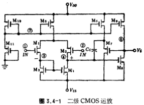
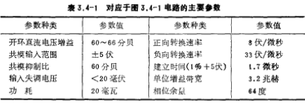
The circuit in Figure 3.4-1 consists of a two-stage amplifier. M1~M4 constitute the differential amplifier of the active load, and M6 provides the working current of the amplifier. M5 and M6 form a common source amplifier circuit, which serves as the output stage of the operational amplifier. M7 is a source follower to overcome the compensation capacitance The feedforward effect eliminates the zero point. M6 provides the operating current to M7. The bias circuit composed of M10 and M11 provides the working current of the amplifier. The threshold voltage of the MOS device in the circuit is ±1.5 volts, and the compensation capacitance
 Pifa.
Pifa.
In the second section, we discussed the design method of CMOS operational amplifier. Here we will discuss the design of the circuit in Figure 3.4-1 and the calculation method of the channel width-to-length ratio of MOS devices.
1. The design of the operating point of the CMOS tube operational amplifier circuit
The potential of node ⑦ in the circuit is determined according to the maximum amplitude of the forward voltage output by the circuit. The output forward swing is 5 volts, and the threshold voltage of the tube is 1.5 volts. To ensure that the amplifier is in the saturation zone, the potential of node ⑦ is 3.8 volts. The negative swing is -5 volts,
For the same reason, nodes ③ and ④ are set at about -5 volts. The potential of node ⑤ can be determined according to the circuit's positive common-mode voltage range. In order to obtain the maximum positive common-mode voltage, the potential of the drain of M5 is about 2 volts.
From the formula (3.3-15), the maximum conversion rate of the op amp is

Here Io is the working current of the input differential stage, which is provided by the M5 current source. Cc is the compensation capacitor, the compensation capacitor of this circuit is 10 picofarads. In order to achieve a conversion speed of 30 volts/microsecond, the current of M5 should be 300 microamperes, which is now about 350 microamperes. The charging and discharging circuit of the compensation capacitor Cc also passes through M7, so the operating current of M6 is also 350 microamperes.
In order to increase the output capacity and drive large capacitive loads, the output stage . The working current is
 . The current source current is twice that of 700 microamperes. M10, M11; the bias current is about 86 microamperes.
In summary, the current ratio of M10, M5, M6, and M9 in the circuit is designed to be 1:4:4:8, that is, the width-to-length ratio of the channel is
1:4:4:8.
2. Calculation of the width-to-length ratio of each MOS tube channel
When designing the layout size of a CMOS circuit, the most important thing is to determine the width-to-length ratio of each MOS tube channel. According to the previous discussion about the working point, the ratio of the channel width to length ratio of each relevant MOS tube can be estimated.
According to the relationship

inferred

Since the current ratio of M10, M5, M6 and M9 is 1:4:4:8, the channel width to length ratio of M5, M6, M8 and M9 is

According to the discussion in Section 2, in order to reduce the input offset voltage of the circuit, the channel width-to-length ratio of M2, M4, M5 and M8, M9 should satisfy the relationship

In the formula, W5/L6, W8/L9 have been determined, as long as W2/L2 is determined, then W3/L3 is also determined.
The quiescent working current and working voltage of M3 and M4 have been determined, as long as the relationship between current and voltage is used,

The channel width to length ratio (W2/L2) and (W4/L4) of M3 and M4 can be determined.
According to the static operating points of M1 and M2, obtain W1/L1 and W2/L2; in this way, the channel width-to-length ratios of all tubes are determined, and their design values are listed in Table 3.4-2.
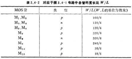
The above calculations have adopted an approximate first-level model. In order to obtain the correct design value, the second-level model of the MOS tube is used for computer simulation to correct the design value.
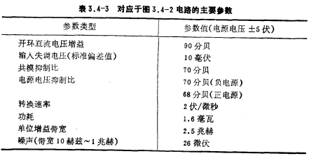
In the circuit in Figure 3.4-1, the output stage works in Class A state, and the currents of M6 and M7 are also large, so the total power consumption of the circuit is large. In order to reduce the power consumption of the circuit, the circuit shown in Figure 3.4-2 can be used, in which the output stages M8 and M9 work in Class A and Class B states.
In order to further reduce the power consumption of the circuit, the circuit also adopts the method of connecting a capacitor in series with a resistor (reducing a source follower) to overcome the feedforward effect of the compensation capacitor. According to the principle mentioned above, the resistance of the series resistance here should be equal to the reciprocal of the transconductance of the second amplifier stage. In the figure, the equivalent resistance between the drain and source of M10 and M11 is used to form the above-mentioned series resistance.
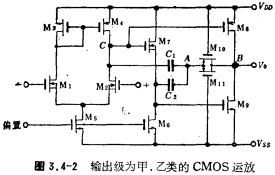
The parameter values of the circuit in Figure 3.4-2 are shown in Table 3.4-3. The voltage gain of the circuit is designed to be higher, about 90 decibels, while the power consumption is greatly reduced.
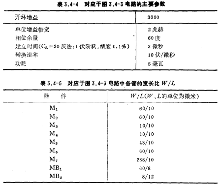
The circuit in Figure 3.4-3 is a CMOS operational amplifier with simple structure and good performance. The compensation circuit does not use zero cancellation, so the second-level transconductance gm1 is required, which is larger than the first-level transconductance gm1. It is now designed as gm1=(5~6)gm1. According to the first-level discussion, the compensation capacitor Cc and the load capacitance The relationship of CL is

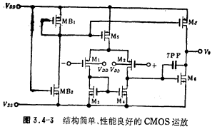
If CL=20 picofarads and gm1=5gm1, then Cc>4 picofarads. Take Cc as 7 picofarads in the circuit.
Under the condition that the power supply voltage VDD is 5 volts and VSS is -5 volts, the parameters of the circuit are listed in Table 3.4-4, and the width-to-length ratio of the MOS device channel is listed in Table 3.4-5.
The circuit in Figure 3.4-4 is a CMOS operational amplifier that works at low voltage and has strong output capabilities. The input stage differential amplifier consists of MN1, MN2, MN6, It is a differential amplifier that converts double-ended to single-ended output. Its output is used to drive the gate of the output stage circuit MP7; MP7 and MN7 constitute the output stage circuit, which is a common source amplifier.
MP7 is a common source amplifier tube, and its load is MN7; the bias circuit is composed of MP1 and MN2. In order to increase the drive capability of the output stage, MOS transistors such as MP2~MP4 and MN5 have been added. Under the action of the input signal, when the output terminal of the differential amplifier ③
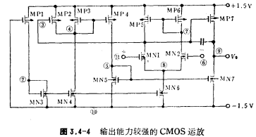
When the voltage increases, the output terminal ⑨ voltage becomes negative; at the same time, MP2 current decreases, MP3, MP4 current increases, node ⑥ voltage increases, MN7 current increases, so when the output terminal is negative voltage, the current flowing into MN7 Increase, enhance the negative output capability. Conversely, when the voltage of node ③ decreases, the voltage of output terminal ③ rises. At the same time, the voltage of node ⑤ decreases, and the current of MN7 tube decreases. Since the output positive current is provided by MP7, most of the current output by MP7 goes to the output load. Only a small part flows through MN7, and as the output amplitude increases, the current flowing into MN7 also decreases, thus increasing the forward output capability. In fact, the MN7 tube can be regarded as a voltage-controlled variable resistor. When the output voltage is positive, the resistance value increases; when the output voltage is negative, the resistance value decreases. The width-to-length ratio of each tube in the figure In Table 3.4-6.
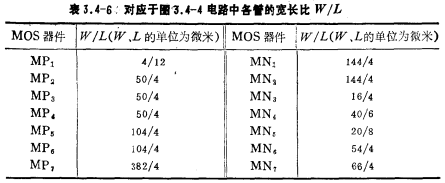
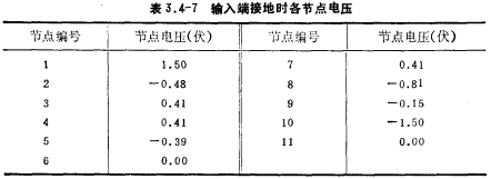
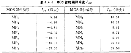
The open loop gain of this circuit is greater than 1000; the unity gain bandwidth is 1 MHz. The DC voltage of each node and the IDS current of each tube are listed in Table 3.4-7 and Table 3.4-8, respectively.
Contact: Mr. Zou
Contact number: 0755-83888366-8022
Mobile phone: 18123972950
QQ: 2880195519
Contact Address: 5C1, Block CD, Tianji Building, Tianan Digital City, Chegongmiao, Futian District, Shenzhen
Please search WeChat official account: "KIA Semiconductor" or scan the following picture to "Follow" official WeChat official account
Please "follow" the official WeChat account: provide MOS tube technical assistance


