Electronic Technology Forum
The basic structure and working principle of charge coupled device (CCD)
Charge-coupled device (CCD) is a new type of MOS device proposed in 1970. It is based on the highly developed integrated circuit planar technology and semiconductor surface theory. Proposed. Although it is called a device, it is not a general discrete device, but an integrated functional device. Because of its simple structure, high integration, and unique functions, it develops rapidly. The working principle of charge coupled device. At present, it has developed into an important branch of large-scale integrated circuits, and its applications are becoming more and more extensive. In terms of numbers, the main purpose is to produce high-digit Shenhang memory to replace the clunky peripheral devices and drums in the computer. At present, 64K and 128K-bit random memories have been produced. The structure and basic principle of CCD will be introduced below, and then its application will be introduced.
1. CCD structure and working principle
1, CCD structure
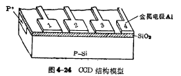
The CCD device is composed of a metal-oxide-semiconductor capacitor array with very small spacing. Figure 4-24 shows the structure model of the N-channel CCD. It is to grow a layer of high-quality silicon dioxide with a thickness of about 100nm on the surface of P-type semiconductor Si, and then evaporate a layer on SiO2 A metal electrode array with a pitch of less than 3μm and a strip length of 4~5μm.
2, CCD working principle
(1) The formation of potential well Everyone knows that MOS The properties of accumulation, depletion and inversion generated on the surface of the semiconductor under the action of an external electric field in the structure are all analyzed from the steady-state process, without considering its transient state. If a pulse voltage is applied to the semiconductor surface, then the transient characteristics of the MOS capacitor and its relaxation process must be considered.
If a sufficiently large pulse voltage (greater than the threshold voltage VT), because there is no high-concentration source-drain diffusion region on the left and right sides under the gate, and there is no source of a large number of minority carriers, a strong inversion layer does not immediately appear on the semiconductor surface. The working principle of charge coupled device. At the moment when the pulse voltage is applied, the holes on the Si surface are repelled, forming a depletion layer. If the pulse voltage applied to the grid is large enough, the thickness of the depletion layer  and depletion layer charge
  will exceed the strong inversion type The thickness of the dot and the amount of charge in the depletion layer, the surface potential will also exceed the surface potential of the strong inversion. We call this and depletion layer deep depletion. At this time, the MOS capacitor is in an unbalanced state. As shown in Figure 4-25(a). When deep depletion occurs, the surface potential is higher than in the equilibrium state. For electrons, the potential energy is lower, and the surface energy level bends more downward. We call this outer depletion layer a potential well. Similar to the situation in the entire region of the PN junction potential, there is a production-recombination center in the depletion region, so electron-hole pairs will continue to be produced. These electrons and holes will drift to both sides under the action of the electric field. Electrons move to the surface, and holes move to the body. These electrons accumulate on the surface and gradually form an inversion layer, and holes accumulate in the body, making the thickness of the depletion layer thinner. After a certain period of time, the MOS capacitor will reach a new equilibrium state. At this time, the thickness of the depletion layer
  and the endless layer space charge area The charge
  is the same as the general MOS transistor in the on state, namely An inversion layer channel with electrical advantages appears on the surface. We call this situation the potential well has been filled. Figure-25(b) shows the clear condition that the potential well has been filled. When the potential well is filled, because the electric field is shielded by the electron charges on the surface, the electric field in the body is weakened, and the potential at the surface also drops, that is, the electron potential energy increases.
There is a relaxation process from the non-equilibrium state to the equilibrium state. In this process, the thickness of the depletion layer under the gate, the surface potential and the MOS capacitance are constantly changing. The time required for this process is related to the generation rate of electron-hole pairs in the potential well, which is also related to the minority electrons at the surface. Life is related. The longer the lifetime of the minority birth, the longer it will take to transition to the equilibrium state. At room temperature, when the young child’s life span is on the order of microseconds, the time from the non-equilibrium state to the mediocre state is about  .
.
CCD is a device that works under unbalanced conditions. If there are no free electrons in the potential well, we say that the potential well is empty, which is called an empty well. In the equilibrium state, the potential well is filled with electrons. We say that the potential well is full, which is called a full well. During the process of the potential well from empty to full, the amount of free charge changes continuously. Therefore, in this process, the amount of charge in the potential well can allow any value from zero to equilibrium. The free charge in the potential well can be generated by itself or introduced from outside. But it must be noted that in the non-equilibrium state, due to the existence rate of the potential well itself, the free charge will increase with time. For example, when the charge injected into the potential well is used to represent information, in order to avoid the interference of the heat generated charges, the information charge cannot stay in a potential well for too long. The working principle of charge coupled device. Generally, it should be much shorter than the time to reach the thermal equilibrium state.
(2) Charge transfer The reason why CCD devices can be applied to large Large-scale integrated circuits can not only form a potential well on the silicon surface under the action of a pulse voltage, but more importantly, the charge in the potential part can be transferred from a potential well to a potential well under the action of a clock pulse. If all voltages are applied to the three adjacent MOS capacitors This section forms a depletion layer as shown by the dotted line, where the third electrode is the deepest and the electron potential is the lowest, the second electrode is next, and the first electrode is the shallowest, as shown in Figure 4-26. If the electron charge is originally stored under the second electrode, since the carriers have the characteristic of transferring to the lower potential energy, then they will transfer under the third electrode. As a result, the stored electronic charge moves one grid position to the right. This is the charge transfer effect of the MOS structure.
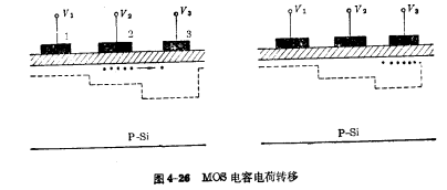
The basic principle of CCD is to store and process information by using the storage effect and transfer effect of the charge in the unbalanced state of the MOS structure.
(3) Charge transfer of three-phase CCD In P-type Si Make a row of MOS capacitors, as shown in Figure 4-27. There are 9 electrodes in the picture, which are driven by clock pulses. Control. Among them 1, 4, 7 are controlled by
 Controlled by 2, 5, 8
 Controlled by 3, 6, 9 by
Figure 4-27 (a) shows the time  The situation of the instantaneous potential well. At this time,
  is at the highest potential
 and
and
Figure 4-27(b) shows the time  a Instantaneous potential well situation. At this time
 ’s potential drops to
 Rising to the highest potential
 , and
, and Still at a low potential
  This , The potentials on the electrodes 1, 4, and 7 are lower than the potentials of 2, 5, and 8, as a result, the potential wells under 1, 4, and 7 are shallower than the potential wells under 2, 5, and 8. Therefore, the electron potential energy under the electrodes 2, 5, and 8 is the lowest, and the electrons in the two potential wells 1 and 7 are transferred to the two potential wells 2, 8 respectively on the right. The potential barriers below 3, 6, and 9 are higher, which not only prevents the electrons from offside to the right, but also prevents the charge from flowing back to the left. Since the original potential well 4 is empty, there is no charge transfer, so the potential well 5 is still empty.
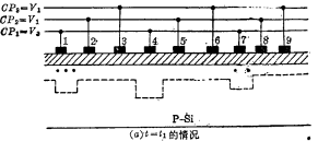
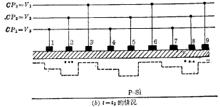
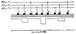
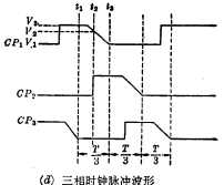

Figure 4-27 (c) means  The momentary potential well situation. At this time,
  drops to the lowest potential
 Still maintain the highest potential
 . In this way, the charge completes the task of shifting the position of the electrode to the right. At this time, the situation of the potential well is similar to Figure 4-27(a), except that the positions of the deep well and the charge have moved one position to the right.
If there is no charge in the potential well to represent the information "1" and "0". Then Figure 4-27(a) shows that the CCD device stores the information "101". In Figure 4-27(c), it means that the information "101" stored in the CCD has moved one grid position to the right. According to the above-mentioned law, the driving pulse is continuously applied, and the information will continuously move from left to right or from right to left. This is the charge transfer method of a three-phase CCD device. In the charge transfer process, one gate transfers charge, one gate accepts charge, and another gate prevents backflow. The working principle of charge coupled device. Therefore, every time a three-phase CCD stores and transfers one bit of information, three grids are required to be controlled in coordination. An N-bit CCD should have 3N gates. Every time one bit is transferred (a total of three gates), the phase of the clock pulse changes by one cycle T, and the time required to transfer one gate is T/3.
The potential well for charge transfer under the CCD gate is also called the channel. Using a P-type semiconductor as the substrate, an N-channel CCD is obtained. On the contrary, using N-type semiconductor as the substrate, the result is a P-channel CCD.
From the above analysis, we know that in the CCD, the coupling between the former and the latter is completely the coupling between the potential wells, and no other connection is required. Therefore, the COD shifts The wiring of the bit register is extremely simple.
3. Information input and output
(1) Information input CCD device input information (also There are usually two methods called "write"), one is PN junction input and the other is photoelectric input. Figure 4-28 (a) (b) respectively show the structure diagrams of these two input circuits.
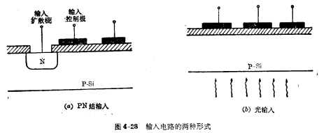
①PN junction input Figure 4-28 (a) is a CCD device For the PN junction input circuit, it makes an N-type diffusion area on the P-type Si substrate, also known as the source of the CCD, and makes a control gate next to the diffusion area. PN junction input can be divided into direct PN junction input and control gate input.
a. When working with direct PN junction input, add a fixed positive bias voltage to the input control gate to form a certain potential well under the gate, and add a larger value to the PN junction The reverse bias voltage makes the PN junction in reverse bias and no carrier injection. If the input information "1" is superimposed on the PN junction input terminal in the form of a negative pulse, the side of the junction between the right side of the PN junction and the potential well under the control gate becomes positive bias , Then the information charge is injected into the potential well below the gate, and is then driven by the driving gate.
b. Control gate input Input PN junction usually adds a small reverse bias voltage, and the input information is connected to the control gate. If writing "1", a larger pulse voltage is applied to the control gate, the amplitude of which is greater than the threshold voltage, so that a potential well is formed under the control gate, and the junction of the PN junction and the potential well becomes forward biased. Then the information charge is injected into the potential well under the control gate.
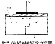
②Photoelectric input The photoelectric input uses the photoelectric effect of the MOS structure. When light shines on a semiconductor, electron-hole pairs will be generated in the potential well and its vicinity. The electrons are stored in the potential well as information charges, and the chamber holes reduce the ionized proper host. As shown in Figure 4-29. In this way, the optical information is converted into electrical information, temporarily stored in the CCD, and then the information is processed by the transfer effect of the CCD. There are two ways of photoelectric injection, either from the back of the sample or from the front. If the light is illuminated from the back, the sample must be thinned to reduce the absorption of the substrate. The working principle of charge coupled device. However, it is more difficult to reduce a large area of Si wafers very thinly. Light from the front, because the metal gate has a shielding effect on light, it is generally used to replace the metal gate with heavily doped polysilicon. When CCD is used for shooting, it uses photoelectric input, and when it is used for information processing and storage, it uses PN junction input.
(2) Information outputFigure 4-30 shows the output of CCD Structure, it includes two control gates (output control electrode and reset control electrode) and two diffusion regions (output diffusion electrode and reset diffusion electrode). There are two ways to read information charge, one is current reading, and the other is voltage reading.
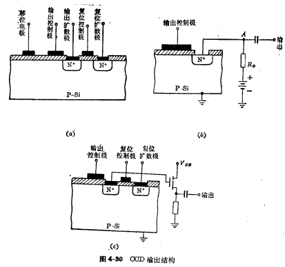
When the current readout method is used, the reset control pole and reset diffuser in Figure 4-30(a) are not used, but a load should be connected in series with the output diffuser Resistor  , the other end of the resistor is connected to the positive pole of the power supply to make the diffusion junction in The state of reverse bias is shown in Figure 4-30(b). When the information charge reaches the diffusion junction, it is collected and a current is generated in the outer loop at the same time. Measuring the voltage change on the load resistance can indicate the amount of charge reached. The output control pole is used to control the amount of charge collected. It often adds a fixed bias voltage much larger than the threshold voltage, but lower than the output diffuser voltage. Although the current readout method is simple, the amount of charge under the CCD electrode is very small, and the amount of free charge in the full well is less than 10-12C. Therefore, the detected signal charge is very small, it must be amplified with a high-sensitivity amplifier, and then connected to the oscilloscope for observation.
In the voltage readout mode, the output diffusion area is connected to the gate of the MOS tube, and the diffusion electrode does not add bias and series resistance, so there is no DC path, as shown in Figure 4- Shown in 30(c). When the detected charge reaches the diffuser, the potential of the diffuser changes, and the initial potential of the MOS tube also causes a change, causing a corresponding current change in the source-drain circuit of the MOS tube. The voltage reading method is more sensitive, because the gate capacitance of the MOS tube is very small, and a small amount of charge can cause the gate voltage to change, so it is easy to detect. When voltage reading is used, a reset electrode must be used. The working principle of charge coupled device. After each charge is detected, a reset positive pulse should be added to the reset gate, and the collected charge will be discharged from the reset diffuser to restore the output diffuser to its original potential. The reset diffuser is often connected to a fixed positive voltage and is at the highest potential of the whole chip.
Contact: Mr. Zou
Tel: 0755-83888366-8022
Mobile: 18123972950
QQ: 2880195519
Contact address: 5C1, CD Block, Tianji Building, Tian’an Digital City, Chegongmiao, Futian District, Shenzhen
Please search the WeChat official account: "KIA Semiconductor" or scan the picture below to "Follow" the official WeChat official account
Please "follow" the official WeChat account: provide MOS tube technical assistance


