Electronic Technology Forum
Analysis and detailed explanation of CCD basic parameters and structure improvement
Basic parameters and structure improvement of CCD
1. Basic parameters
There are many factors involved in the basic parameters of CCD, some of which are interrelated, so it is impossible to analyze and discuss them in detail here. The following only briefly introduces the concepts of some parameters. The main performance parameters of CCD include threshold voltage, charge transfer efficiency, operating frequency range and load capacity, etc.
(1) Threshold voltage
It has the same meaning as MOS transistors.
(2) Charge transfer efficiency
The charge transfer efficiency refers to the percentage of charge transfer when the information charge is transferred from one potential well to the next. Basic parameters of CCD MOS. This is a basic parameter that determines the performance of a CCD device. People always hope that the higher the transfer efficiency, the better. But just as it is impossible to pour water 100% from one container to another, so it is impossible for electric charges to transfer from one potential well to another without loss. The loss in the charge transfer process is mainly due to the surface trap effect, and all the divided charges are captured by the traps, resulting in a decrease in transfer efficiency. If the transfer efficiency is low, it limits the number of units that can be transferred, thereby limiting the resolution of the device.
(3) Operating frequency range and dynamics
MOS shift register is similar, with low frequency limit and high frequency limit. The upper limit of the operating frequency is mainly limited by the efficiency of charge transfer. Because the higher the operating frequency, the lower the transfer efficiency. At the same time, it is also related to the number of digits of CC D. If the number of digits is too large, a certain amount of charge can be obtained at the output terminal only by reducing the frequency of use. Therefore, to increase the operating frequency, the CCD is first required to have a higher transfer efficiency. The lower limit of CCD working efficiency is determined by the process of heat generation, which is determined by the lifetime of carriers. The longer the life, the longer the charge storage time, so the lower limit of the operating frequency can be lower.
The operating frequency range of an ordinary three-phase CCD is approximately between kilohertz and megahertz.
(4) Charge load
The charge load is the amount of free charge that can be contained in the potential well, and it reflects the output capacity. The negative maximum amount of charge is related to the area of the electrode, the thickness of the oxide layer, and the working voltage. The larger the electrode area, the thinner the oxide layer and the higher the electrode voltage, the greater the charge load.
II. Introduction to improved CCD structure
(1) Disadvantages of the original CCD structure
Three-phase CCD is the earliest developed structure, and its biggest feature is its simple structure.
It can be achieved with fewer process steps, but it is not practical due to the following shortcomings.
①Electrode gap If the electrode gap is wide, under the electrode gap The transmission channel will form potential gold, which seriously hinders the transfer of charge. Basic parameters of CCD MOS. Therefore, it is desirable that the electrode gap be as narrow as possible. Generally, it is required to be less than 3μm, which is limited by the photolithography process. Secondly, the potential under the electrode gap is fully formed, which is also related to the charge distribution in the oxide layer. This charge distribution is difficult to control with current technology. Third, the electrode gap is very sensitive to external influences, and even human breathing can change the distribution of potential energy under the electrode gap, thereby changing the performance of the device. The thin oxide layer at the electrode gap is often exposed to the air, which is greatly affected by the environment and is easily contaminated.
②The electrode leads cross In order to ensure the directional movement of the information charge, it is required The potential well is inclined, so a three-phase clock pulse must be used, which will cause the electrode leads to cross, and tunnel leads have to be used, which brings difficulties to the wiring.
③The transfer efficiency is reduced and the working frequency is limited Because the information charge is along the surface During the transfer process, to be captured by the surface traps will reduce the transfer efficiency and limit the operating frequency.
(2) Improvement of CCD structure
In order to overcome these shortcomings, the CCD structure must be improved. Two improved structures are introduced below.
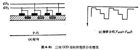
①Two-phase CCD Figure 4-31 shows the two-phase CCD structure, which is a double-layer electrode structure. The polysilicon electrode is sandwiched between SiO₂, and the aluminum electrode is on top. They are arranged in order. This structure can be driven by a two-phase clock. When driving with a two-phase clock, connect the adjacent pair of upper and lower electrodes in parallel. In Figure 4-31(a), the lower electrode is on the right, so the potential well on the right is deeper, and the charge can only be transferred to the right. Figure 4-31 (b) shows the clock pulse The voltage is greater than
 Potential well distribution.

After this improvement, the electrode spacing is equivalent to zero, which overcomes the difficulty of reducing the electrode spacing in the basic CCD process, and greatly improves the transfer efficiency; in addition, the potential well is from left to The right is tilted, allowing the information charge to move in a single direction.
From the structural layout, the two-phase CCD is much simpler than the three-phase CCD.
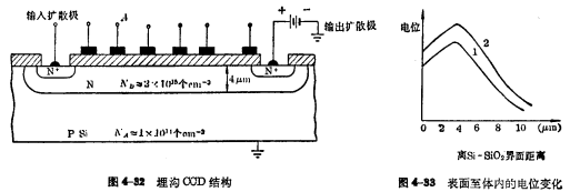
②Buried trench CCD In order to overcome the impact of the semiconductor interface state on the CCD device Due to the adverse effects, the active area of free electric charges is far away from the surface, and a buried trench CCD has been developed. Basic parameters of CCD MOS. Figure 4-32 shows the structure principle of buried trench CCD. It uses ion implantation or diffusion to introduce a low-concentration N-type impurity layer that is opposite to the conductivity of the substrate on the P-type substrate, and produces high-concentration input and output on both sides of the N area. N+ area. When working, the output diffusion area is connected to the highest potential, so that the PN junction is in reverse bias, and the N area is at a positive potential at the same time. If the control gate is at ground potential, it is equivalent to applying a negative voltage to the control electrode for the N region, so that a certain depth of depletion layer is generated on the surface. On the other hand, the PN junction in the reverse bias produces a second depletion region. If the voltage of the output diffuser is as large as 30~40V, the depletion layers on both sides must be connected. Make the N area under the electrode become the depletion area. The potential distribution from the surface to the P-type region is roughly as shown in the curve in Figure 4-33. It can be seen that in the place away from Si-Si02interface 2~3μm, the potential The highest, that is, the lowest potential energy of the electron is not in the interface, but in the body. In this way, the channel of electronic activity is buried in the body, and the avoids the influence of the interface on the free charge.

If the potential of the transfer electrode A is increased, the potential at 2~3μm from the surface will increase, and the electron potential energy will be lower, and the charge under the adjacent electrode will move to the lower part of the A pole. Potential well transfer. The main advantage of this device is: because the charge is transferred away from the interface, the loss of signal charge caused by the trapping of the interface state can be reduced. Since the mobility of carriers in the body is higher than that of the surface, and there is a larger drift electric field in the channel, the transfer speed of the charge is faster, so the transfer efficiency and operating frequency are higher, and the maximum operating frequency can reach 100MHz. This buried trench CCD memory has a transfer efficiency at 2~5MHz. Up to 99.9999%. The highest operating frequency of the aforementioned surface CCD is only about 10MHz. Its main disadvantage is that the potential well is relatively shallow and the charge carrying capacity is small.
Contact: Mr. Zou
Tel: 0755-83888366-8022
Mobile: 18123972950
QQ: 2880195519
Contact address: 5C1, CD Block, Tianji Building, Tian’an Digital City, Chegongmiao, Futian District, Shenzhen
Please search the WeChat official account: "KIA Semiconductor" or scan the picture below to "Follow" the official WeChat official account
Please "follow" the official WeChat account: provide MOS tube technical assistance


