Electronic Technology Forum
MOS read-only memory (ROM) working principle and characteristics of the reading and writing process
MOS read-only memory (ROM)
Read-only memory is a memory that stores fixed and unchanging information. It can store fixed constants, fixed functions, fixed instructions, and so on. When in use, these fixed contents can only be read out, and new information cannot be written at any time, so this kind of memory is called a read-only memory. At present, this kind of memory is widely used in microprogram sequence generators, computer hard-arranged subprograms, data tables, random control logic, decoders, letter or character generators, etc. Because the circuit structure of ROM is simpler than RAM, it develops relatively rapidly. MOS structure ROM occupies a very important position in semiconductor integrated circuits, and there are many varieties. According to the development process, it can be roughly divided into mask programming ROM and programmable ROM.
Mask programming ROM is a mask designed according to user requirements to program the program, and the program is fixed at the time of manufacture. The most eye-catching thing at present is the programmable ROM, its write data can be changed arbitrarily. Of course, its rewriting process is more difficult than RAM. Most of this kind of ROM uses the characteristics of the gate insulating layer of the insulated gate field effect transistor to store charges to write signals, but it is mainly used for reading, so this kind of memory is called the main read memory. In addition, because the written data can be kept for a long time without missing, it is also called non-volatile memory.
The following will introduce the structure and principle of the masking program read-only memory and the output selection level programmable read-only memory logic array.
1, MOS mask preparation program ROM
This is the most basic read-only memory. Because the mask programming program is fixed with a mask during manufacturing, the data input is five The relationship between superiority and output cannot be changed. Once the product is made, the program cannot be re-adapted. This kind of memory stores logical information "1" and "0", which is determined by whether the transistor under the mask is turned on or off.
Figure 4-11 shows a 4×4 MOS mask program ROM. It is composed of ROM matrix, decoder, output selection circuit and buffer. The pre-programmed content is stored in the ROM matrix. The matrix in the figure is composed of 4 rows and 4 columns. If there is a MOS tube at the intersection of a row and a column, it means "1" is stored, and a place where there is no MOS tube means "0" is stored. The content stored in the matrix in the figure is:
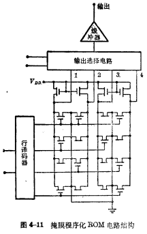

The row can be addressed by the row decoder, all MOS transistors on the addressed row will be turned on, and the information will be passed to the output selection circuit. However, which of these information can be output is also controlled by the output selection circuit. The output selection circuit can select any cell in the matrix (that is, the intersection of rows and columns). The information stored in the selected unit is output after being amplified by the buffer. The output information in the circuit is controlled by the output selection circuit and output one by one. This output method is called serial output.
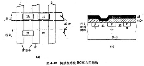
Mask programmed ROM can be made using typical P-channel enhanced technology. Figure 4-12 (a) shows part of the structure of the storage array. As can be seen from the figure, where the aluminum strip crosses the bit line and ground line diffusion strips, a MOS transistor can be formed. The three blocks 11, 12, and 21 between the diffusion bars are made of thin oxide layers, and the other places are thick oxide layers. In this way, when a pulse is applied to the aluminum bar, the MOS tube under the thin oxide layer is turned on, while the MOS tube under the thick oxide layer cannot be turned on. If it is specified that the conduction is "1", the non-conduction is "0". Therefore, the information of this kind of ROM is pre-made in it, and once it is made, the stored content will not change.
The actual ROM integration is relatively high. According to actual needs, it can generally range from a few hundred to tens of thousands.
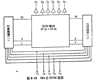
Figure 4-13 is a block diagram of a 324-bit medium-scale ROM, which is a part of a desktop computer. In the middle of the figure is a 324-bit matrix with 27 rows and 12 columns. On the left and right are two 5-input decoders, with the help of two decoders, any row can be addressed. There are 6 output buffers arranged on the upper part, which amplify the read signal and output it.
 < br/>
Mask programmed ROM can be used as a storage unit with only one MOS tube, so it has the advantage of high integration; since writing is not considered, the circuit structure and process It is much simpler than RAM and has a higher yield.
2, programmable read-only memory
Programmable read-only memory is developed on the basis of fixed ROM. Generally, a fixed ROM cannot be changed once its storage content is established. This is subject to certain restrictions in use. Programmable read-only memory, its storage content can be programmed according to needs. If there is a new need, the original content can be "erased" and new content can be compiled, which has greater flexibility and wider application. MOS type programmable read-only memory can be divided into two categories in terms of performance:
①Electrically programmable read-only memory (EPROM)
This type of memory can use ultraviolet light or  Radiation will erase all stored content at once, and then write new content.
②Electrically rewriteable programmable read-only memory (EAROM)
This type of memory can use electrical methods to erase the stored content word by word, and then rewrite it to rewrite it word by word. So it has the function of RAM, but the writing energy is large, the reading and writing speed is slow, especially the writing speed is slow, so it is still used as a read-only memory. It is more flexible and convenient than EPROM. If its erasing and writing energy is reduced, and its reading and writing speeds are increased, the non-volatileness of semiconductor RAM can be realized and the magnetic core can be completely replaced.
MOS-type PROM can be divided into two types in terms of structure: One type is a polysilicon microgate electrode, and a thin silicon dioxide layer is used as a sugar medium for floating gate avalanche implantation. MOS structure (FAMOS), EPROM can be constructed with such devices. On the basis of the above, there is also a stacked gate implanted MOS structure (SIMOS), which can form EPROM or EAROM. The other is a composite gate dielectric MOS structure, which is a MOS type device that uses a double-layer material of silicon nitride-silicon dioxide or aluminum oxide-silicon dioxide as the dielectric and aluminum as the metal gate electrode. They can Forms EAROM. The following will introduce their structure and working principle respectively.
(1) Floating gate avalanche injection MOS programmable read-only memory
Figure 4-14 (a) shows the storage unit of this kind of memory, which consists of two tubes. Where  It is an ordinary MOS tube, which plays a control role;
  is a floating leak MOS tube plays the role of storing information. We stipulate that
  is the storage information "1" when it is turned on,< img src="/userfiles/images/2020/11/17/2020111710189525.png" title="image.png" alt="image.png"/>The storage information is "0" at the end.
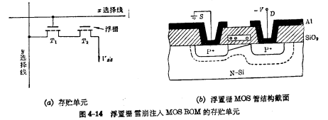
Most of the floating gate avalanche injection MOS programmable read-only memory MOS transistors use P-channel technology, and the floating gate is made of polysilicon, suspended in The middle of SiO2 is called floating gate MOS transistor, as shown in Figure 4-14(b). Here is how it works.
If the source and drain are both connected to 0 level, there is no charge on the polysilicon floating gate, and there is no conduction between the source and the drain.
If the source is grounded and a sufficiently high negative voltage is applied to the drain, then the polysilicon floats will form a positive potential on the drain coverage area. Therefore, under the action of a strong electric field, the edge strip of the leakage diffusion zone will first have an avalanche multiplication effect, and some of the hot electrons that have obtained a certain kinetic energy can cross the Si-SiO2 interface The barrier enters the polysilicon gate in silicon dioxide, as shown in Figure 4-15. Since electrons are captured on the floating shed, a negative voltage VG (VG is a negative value), when |VGl>|VT l, an inversion channel is formed on the Si surface under the gate to make the tube in the on state, corresponding to the signal "1", if there is no avalanche, there is no charge in the silicon gate, and the MOS tube is off. Status corresponds to the signal "0".
If the SiO3 layer between the polysilicon and the silicon substrate is 100nm, the resistivity of the material substrate When it is 5~8Ω•cm, the avalanche multiplication effect occurs when the PN junction between the drain and the substrate is about -30V. At this time, the charging current to the floating gate can reach 10-7A/cm2order of magnitude. The amount of charge transferred to the floating gate is related to the magnitude and duration of the applied voltage. Such as , the electrons injected into the floating gate in about 10ms can reach 4×10¹² pcs/cm2After the electrons are injected into the polysilicon gate, the energy is sharpened due to scattering, and the electrons It stays on the silicon gate stably and can be maintained for a long time. Someone has done an experiment and found that 70% of the information charge can be maintained for 10 years at 125°C.
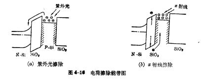
If the stored information charge needs to be eliminated, energy should be given to the electrons so that the electrons can jump over the silicon dioxide barrier gold and return to the Si substrate. The memory is irradiated with ultraviolet light, and after the electrons on the floating gate obtain photon energy, they can pass through the SiO2 barrier and return to the Si substrate. Or you can use  Radiation. If the energy of
  is greater than the forbidden width of silica, it can be generated The electron-hole pair, the holes enter the floating gate, neutralize the electrons in it, and realize the function of erasing the original signal. This method of clearing signal charges is called optical clearing, as shown in Figure 4-16.
 < br/>
Although the circuit is exposed to various rays of radiation in the atmosphere during use, since the dose of this radiation is very small, it will not affect its storage Function.
Figure 4-17 (a) is the circuit diagram of the FAMOS read-only memory with N rows and M columns storage matrix, and (b) is its read-write control circuit. The following briefly introduces its reading and writing methods.
When writing, connect VDD to a larger negative voltage (such as -45V), At the same time, the write control voltage Vp is applied to turn on the Tp tube. If you write "1", add "1" voltage to the input terminal to make Turn on, and in
 Select the line to apply a negative voltage to the storage unit
 on. At this time, the larger negative voltage VDD will pass
 The drain of the tube causes an avalanche breakdown and will Hot electrons are injected into the floating gate. In this way, "1" is written into the cell. To write "0", use
 < span style="font-size: 16px;">The tube remains cut off, and the negative voltage VDD cannot be applied to the FAMOS tube of the selected unit. Charge injection. When writing, the chip selection signal
 Make the read-and-play circuit inoperative, that is, it can only be written, not read.
When reading,  The tubes are all cut off, and a smaller power supply voltage VDD (about- 15V), then the load tube
  and the storage unit form a gate Circuit, if the chip select signal
  turns on the read and amplifier circuit, then The signal stored in the unit can be read out through the read-and-play circuit.
(2) Stack gate injection MOS programmable read-only memory
Floating gate type memory cannot erase the stored information with electricity, which is not convenient to use. Therefore, the MOS read-only memory with overlapping gate structure has been further developed, which can be erased and programmed by electricity. It can not only be made into an erasable programmable read-only memory (EPROM), but also an electrically rewritable programmable read-only memory (EAROM).
①Basic schematic diagram
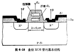
4-18 is the basic junction gate of stacked gate MOS, which is an N-channel device made of P-type substrate. Different from FAMOS devices, there is an extra layer of control gate electrode on the silicon gate. The lower floating gate has the same function as the FAMOS device, which stores signal charges; the upper control gate is the same as The decoder is connected, and the unit is selected when reading, programming and erasing The role of. The storage unit uses only one stacked gate MOS tube, which further improves the integration level of the circuit.
 < /span>
In the device with this structure, the electron injection into the floating gate is not done by the avalanche multiplication effect, but by the "channel injection". The so-called channel injection is to add a sufficiently high voltage between the drain and the source to make the electrons accelerated by a high electric field into hot electrons. When the energy exceeds the barrier height of the silicon dioxide-silicon interface, the additional positive on the control gate Voltage, electrons are injected directly into the floating gate from the channel. In order to achieve a sufficiently high channel electric field, the channel length must be sufficiently short. Usually when the source-drain voltage is 20V, the channel length should be less than  .
.
What kind of signal is stored in the unit depends on whether there is charge in the floating gate. The presence or absence of charge in the floating gate directly affects the change of the valve voltage on the control gate. It is easy to understand that when there is no electronic charge on the floating gate, it does not have any effect on the channel. The quotient voltage of the device is small, but when a large amount of electronic charge is stopped on the floating gate, the negative electric field formed will cause the The P-type becomes enriched in the surface layer, which greatly increases the threshold voltage of the device. Ruling represents the reading voltage when there is no charge on the floating gate, so the information stored in the cell can be judged by the size of the threshold voltage. The erasing of this kind of device can also be realized by ultraviolet light irradiation.
② Improved EAROM reading and erasing operations
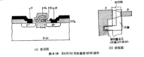
Figure 4-19 shows the actual stacked gate MOS device using the improved EAROM memory cell, which is slightly different from the above-mentioned basic structure. This improvement is to achieve electrical rewriting. It not only erases every time, but also selects to erase word by word. Its floating gate does not completely cover all the channel area, and there is a small coverage area on the source other than the channel. This coverage area is used for erasing data, and the oxide layer below it is relatively thin, about 40~50nm, which is called the erasing area. A part of the control gate overlaps the floating gate, and the other part covers the area not covered by the floating gate.
The following is a brief introduction to the process of programming, reading and erasing.
Figure 4-20 shows the storage matrix of BAROM. In the picture  Connect the wire to the control grid,
  Select the wire to connect to the drain, and program When erasing, all sources are connected to the ground potential. When erasing, all sources are connected to the erase potential.
 .
.
a. Programming operation
Connect the source of all devices to ground, and connect the control gate and drain of the selected cell to a programming voltage that is large enough to make the channel that can cross the silicon dioxide-silicon barrier Hot electrons are injected into the floating gate. As a result, the valve voltage of the stacked gate MOS drifts in a large direction, such as increasing from 1V to 10V. This puts the signal "1" into the unit. In the device shown in Figure 4-19, the funnel-shaped channel can increase the current density near the retention to improve the injection efficiency. If there is no charge in the floating gate, the equivalent valve voltage of the control gate , it is considered that the signal stored in the unit is "0".
b. Read operation
In the selected cell On the selection line (control grid), add the readout voltage
 , and meet
 . At this time, the selected cell that is not programmed ("0" state) is turned on, and current flows through the bit line, while the programmed ("1" state) selected cell is in the off state, and no current flows through the bit line. , You can distinguish the data stored in the memory.
2, erase operation
Erasing can generally be accomplished by two mechanisms. That is to neutralize the electrons in the floating gate, or directly emit the electrons in the floating gate. The method of electrical erasing does not have the "self-limiting" effect of optical erasing, and will produce transition compensation (that is, the floating gate is positively charged). However, because a part of the channel of the stacked gate MOS tube is not controlled by the floating shed, the transistor will not appear depleted.
If the entire array is erased, the erase voltage Add on the common source line S, all word lines
 are grounded, and electrons can be directly emitted to the source through a thin oxide layer. If the selected cell is erased and the word line of the selected cell is grounded, a positive voltage of 25V is applied to the word line of all unselected cells. Erase voltage
  via
via  The decoder is added to the bit line (that is, on the drain) of the selected cell, through
  Cross overlap of selection lines to achieve selection erasure. In order to prevent unselected cells from generating channel charges, the common source line S should be in a floating state.
(3) MIOS type electrically programmable read-only memory
MIOS type electrically programmable read-only memory, its storage device is composed of metal-insulating layer-silicon dioxide-silicon. The insulation layer currently uses  Two materials. If using
  , this storage device is called MNOS type Non-volatile memory; when using
  as an insulating medium, it is called It is a MAOS type non-volatile memory. Generally, the bottom of the MNOS structure uses N-type Si, and the substrate of the surface MAOS structure uses P-type Si, as shown in Figure 4-21.
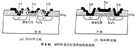
The difference between this device and ordinary double-layer dielectric field effect transistors is SiO. The thickness of the film is very thin, only two to a few nm. The MIOS type memory uses a certain gate voltage to act on the Si surface, so that the carriers in the silicon pass through the thin SiO with a certain tunnel effect2 , And store it in  or
or  in the trap of the interface to achieve threshold voltage Change, so as to achieve the purpose of storing information. Take the MNOS programmable read-only memory as an example to illustrate the working principle of writing and reading.
In Figure 4-21(a), when the substrate and the gate are grounded, and the source and drain are connected to the same negative potential, surface breakdown occurs at the source and drain junctions . The resulting avalanche current makes the potential at the bottom of the gate the same as the drain-source. As a result, the electrons in the substrate pass through the thin silicon dioxide and enter the silicon nitride due to the tunnel effect, due to  Interface and
  There are traps with higher density in the body, so electrons are stored in the traps. Because there is a negative charge in the gate medium, the valve voltage moves in the positive direction. This process is usually called writing "0". At this time, the threshold voltage is VT O means. On the contrary, when the source and drain are at ground potential and the gate is connected to a negative voltage, electrons are emitted from the gate dielectric to the substrate, and the valve voltage moves in the negative direction. This process is called writing "1", and the valve voltage uses
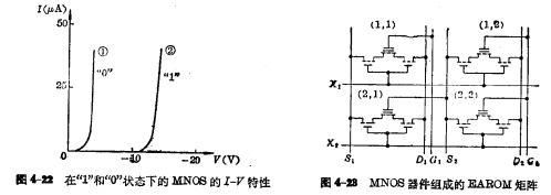
  means. Figure 4-22 shows the I-V characteristics of the MNOS device. The first line represents the storage of the "0" signal, and the second line represents the storage of the "1" signal.
 < /span>
Figure 4-23 shows the EAROM matrix composed of MNOS devices. Each storage unit is composed of three tubes, with an MNOM tube in the middle, and a common MOS tube connected in series on both sides. Their grids are all connected to  Decoder, as the selection control tube.
①Write operation If you want to write "0" into the unit (1, 2), enter the  Add negative potential online (- 35V), all other lines are grounded. At this time, the two MOS tubes in the (1, 2) unit are turned on, so that the source and drain of the MNOS tube are respectively connected with S2 and D2 line is connected, and an avalanche occurs. Hot electrons are injected through the tunneling effect
 Interface and
 In , the valve voltage of the tube is moved in the positive direction, and "0" is stored in it. If you want to write "1", you can go to
 < span style="font-size: 16px;">The line is connected to a negative bias voltage, and the remaining lines are grounded. At this time (1, 2) the source and drain of the MNOS tube in the unit and
 and
and The wire is connected to ground potential. The trapped electrons in the silicon nitride are emitted into the silicon substrate through the tunneling effect, causing the valve voltage of the tube to move in the negative direction, and "1" is written into the cell.
②Read operation in  Apply a negative voltage to the line to turn on the two MOS transistors, in
  Add and read the voltage online
 , you can read the stored signal.
The working principle of MAOS programmable read-only memory is similar to MNOS. The difference is  There are generally more acceptor electronic traps. So regardless of whether the grid is positive or negative, the
  interface only Can cause the storage of negative charges. Generally, when a positive pulse is applied to the gate, the charge storage process is basically the same as that of the MNOS device. That is, when a positive pulse is applied to the grid, there is an electron charge storage. On the contrary, when a negative pulse is applied to the gate, the electrons return to the surface of Si and the charge is removed. In another case, when a negative pulse is applied to the gate, electron injection may also occur (inject electrons from the metal gate to the trap), but when the negative gate voltage increases to a certain level, SiOThe electric field in the 2 layer becomes stronger, and the electrons in the trap will be driven out, passing through the SiO2 layer and entering the Si body, Make the signal clear.
In the above, we have introduced the floating-gate and dual-dielectric memory respectively, and then compare their similarities and differences. Their common point is non-volatile memory, and the working principle is similar. They are all through injecting charges into the dielectric film. These stored charges change the threshold voltage of the device, and use different threshold voltages to change the threshold voltage of the device. Represents different storage signals to achieve the function of completing storage. But compared with the two; there are the following main differences:
①The location of signal charge storage is different
Floating gate device charge is stored on the floating gate in the dielectric, while dual dielectric device charge is mainly stored in the trap at the junction of two different dielectrics. For example, in  There are a large number of carrier traps at the interface. These interface traps are places where carriers are stored.
②The charge injection and removal mechanisms are different
Floating gate devices mainly use avalanche breakdown to achieve hot carrier injection, while dual dielectric devices mainly use ultra-thin SiO2 layers (2~ 4nm) carrier tunneling effect, inject charge into the trap at the interface of the two media.
③The writing energy, speed and signal hold time are different
Because the SiO2 layer under the floating gate of the floating gate device is relatively thick, the writing energy is relatively high. High, the writing speed is slower, but the information retention time is longer, and due to the silicon gate self-alignment process, the readout speed is faster, similar to ordinary MOS transistors; while the dual-dielectric device is in  SiO2 is extremely thin, so the writing energy is low, the writing speed is fast, but the signal retention time is not as long as the floating gate memory; and it is not easy to use self-alignment technology , So the reading speed is slower. Especially the durability is four to five orders of magnitude lower than that of the floating gate type.
Contact: Mr. Zou
Tel: 0755-83888366-8022
Mobile: 18123972950
QQ: 2880195519
Contact address: 5C1, CD Block, Tianji Building, Tian’an Digital City, Chegongmiao, Futian District, Shenzhen
Please search the WeChat official account: "KIA Semiconductor" or scan the picture below to "Follow" the official WeChat official account
Please "follow" the official WeChat account: provide MOS tube technical assistance


