Electronic Technology Forum
MOS integrated circuit functions and measures considerations from the perspective of circuit design
When looking at MOS integrated circuits from the perspective of circuit composition, we must first compare with the past transistors and bipolar integrated circuits, fully understand the inherent characteristics and shortcomings of MOS integrated circuits, and fully study how to select suitable circuits and circuit methods. Looking at the characteristics of MOS integrated circuits from the perspective of digital circuit design, the following can be cited.
(A) Because there is no need for isolation, the structure of MOS transistors can be very simple; MOS transistors can be used to form high resistance; and the storage function of the gate of MOS transistors can be used, and the storage circuit can be realized with few structural elements. For the above reasons, the integration level of the MOS circuit can be made very high. Especially in terms of shift registers with unlimited number of pins, MOS circuits can give full play to their characteristics. MOS tube circuit design.
(B) Since the gate of the MOS transistor has a storage function, a storage distribution logic circuit can be used.
(C) The manufacturing process is simple and the price can be lower.
(D) The input impedance is high, so the fan-out is large. In turn, it is easily affected by induced noise. The output impedance and input and output capacitance are large, so the switching speed is slow.
(E) The input and output logic levels are very different, so the noise tolerance is large, and the margin of the circuit structure is large.
(F) Low power consumption is expected. Especially when the load MOS transistor is driven by a clock or a complementary structure, the power consumption can be reduced to an extremely low level.
(G) The amplification is small, so the switching characteristics are easily affected by stray capacitance, current load, etc.
(H) Consider the electrostatic damage. Therefore, special protective measures should be taken.
The desktop computer is the most suitable machine to use MOS integrated circuits, and it has made great progress. Now take this kind of computer as an example to discuss the application of MOS integrated circuit circuits.
The arithmetic register part is usually composed of a serial synchronous shift register, which is one of the components that can best play the function of MOS integrated circuits. MOS integrated circuit shift registers are highly integrated, and dual 8-bit shift registers, dual 16-bit, 48-bit, 64-bit and higher-integration shift registers have been successfully developed.
The arithmetic device of a desktop computer is an addition and subtraction device, which is usually composed of a full adder, a carry or borrow signal detection circuit, and a two-decimal circuit. The structure of MOS integrated circuit suitable for adder and subtractor is shown in Figure 3.4. Figure 3.4 (a) is a bitwise addition logic circuit composed of ordinary gate circuits, a1a2, represents a pure binary number that should be added, and C represents a carry or borrow, which causes a MOS integrated circuit. Figure 3.4 (b The logic circuit shown in) uses the transfer form of the input signal between the gate and the source of the MOS transistor as the basic circuit. This basic circuit is composed to form an adder circuit, without the need for an inverter that takes the complement of the input signal. , The circuit can be simplified, the signal transfer time is also shortened, in addition, it also has the characteristics of fewer leads and fewer components.
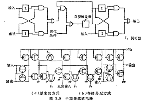
The dynamic storage function of MOS integrated circuits can be used to form storage allocation logic, and the introduction of this logic can also simplify the circuit. Figure 3.5 gives an example of a half adder. Connecting the temporary storage part of the flip-flop in Figure (a) with the gate function, the circuit can be simplified. MOS tube circuit design.

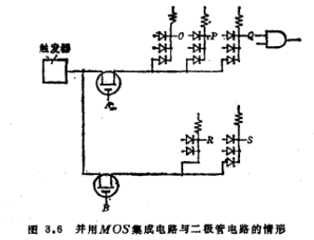
The program device and the judgment device are usually composed of gate circuits and flip-flops, but the gate circuit is limited by the number of leads, and the integration cannot be raised very high, so a large reduction in cost cannot be expected. At the same time, considering the large noise tolerance of MOS integrated circuits, in order to achieve design economy, in the stage of small-scale integrated circuits, MOS integrated circuits and diode gate circuits are used in combination. An example is shown in Figure 3.6.MOS管电路设计。

The following explains the matters that should be paid attention to when using MOS integrated circuits for circuit design.
(1) Logic level
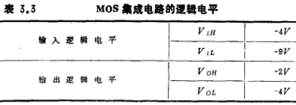
There are currently several types of input and output logic levels for MOS integrated circuits. Table 3.3 shows an example of the logic level specifications.
Now take a look at the situation in Table 3.3. Pay attention to the load conditions when the MOS integrated circuit is DC-coupled. If the output logic level meets the specifications in the table, there is no problem. However, if a diode gate circuit is used in combination, when using a MOS transmission gate, it is necessary to fully consider the diode and transmission gate. The level shift and the level change caused by the load resistance are designed for level distribution. The external equivalent additional resistance in Figure 3.6 is the parallel value of OPQRS. These resistances can usually be specified within the range that meets the load condition specification. On the other hand, if the level shift in the diode and the transmission gate are 0.5V and 1V, respectively, The noise tolerance can be estimated as 4V-(2V+0.5V+1V)=0.5V.

(2) Transmission delay
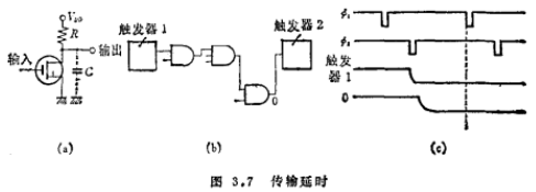
For MOS integrated circuits, the switching speed is relatively slow, especially the turn-off delay is large. Now consider the inverter circuit of Figure 3.7. The cut-off switching time is determined by the load resistance R and the output capacitance. The time constant of the capacitor C composed of the secondary input capacitance and wiring capacitance is determined. Let us study the propagation delay of the circuit in Figure 3.7(b). As shown in figure (c), to make the output level of the final gate reach the specified logic level before the trigger write clock ф2, R and C must be greatly reduced, especially the number of gate stages.
(3) Temperature change and power supply change
Temperature and power changes cause parameter changes inside MOS integrated electric nozzles, most of which are non-linear factors. Leakage inside integrated circuits is a typical example. In addition, when a diode is used in combination, there will be changes in parameters such as internal leakage. Changes in these parameters often bring unexpected inconvenience. Therefore, changes in temperature and power supply should be fully considered in the initial design. MOS tube circuit design.
(4) Measures to be taken against electrostatic damage
As mentioned earlier, MOS integrated circuits have troublesome problems such as electrostatic destruction. Although a protective diode is added to the input terminal of each MOS integrated circuit, the actual applied voltage is often higher than the original estimated range. When designing the whole machine using MOS integrated circuits, measures should be taken to prevent electrostatic damage. For example, when several printed circuit boards are used to form a system, the lead terminals of each printed circuit board must not be open, and a resistor should be connected between the terminal and the ground to form a closed loop. At the same time, some measures should be taken. For example, the casing of the machine is not made of metal. Or a machine made into an inorganic shell, etc.

Contact: Mr. Zou
Contact number: 0755-83888366-8022
Mobile phone: 18123972950
QQ: 2880195519
Contact Address: 5C1, Block CD, Tianji Building, Tianan Digital City, Chegongmiao, Futian District, Shenzhen
Please search WeChat official account: "KIA Semiconductor" or scan the following picture to "Follow" official WeChat official account
Please "follow" the official WeChat account: provide MOS tube technical assistance


