Electronic Technology Forum
Example analysis of DC amplifier circuit of MOS transistor chopper
The MOS transistor chopper amplifier circuit generally has the structure shown in Figure 2.126(a). In order to remove the mains frequency noise and other high frequency noise superimposed on the input signal, a low-pass filter can be added to the input. The signal modulated by the chopper is amplified by an AC amplifier, detected by a synchronous detection circuit, and then smoothed by a low-pass filter and output.
Generally, in order to further improve the overall nonlinearity and stability, the method of adding negative feedback as shown in Figure 2.126 (b) and (c) is often used.

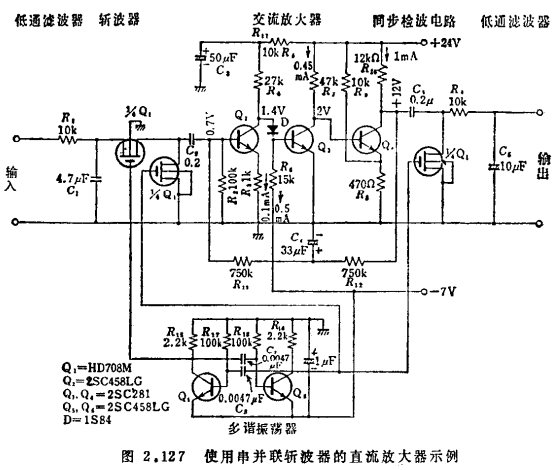
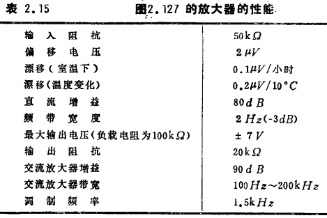
Figure 2.127 is the specific circuit. R1 and C1 constitute a low-pass filter at the input. In the integrated circuit device HD708 containing four MOS transistors, two of the tubes are used for the chopper, and the other tube is used as a synchronous detection switch. Q2~Q4 are DC-coupled AC amplifiers. The collector voltage of the primary Q2 is 1.4V, which is coupled to the base of Q3 through a diode D. MOS transistor chopper amplifier circuit. The collector of Q4 adds DC negative feedback to the base of Q2 via R12 and R13 to stabilize the operating point. The AC component of the feedback loop is bypassed by C4, so negative feedback cannot be added in the modulation frequency band. Q5 and Q6 are multivibrators driving the chopper and synchronous detection switch, and the driving voltage is 1.5kHz. The pinch-off voltage of HD708 is about -2~-5V, so a drive voltage of 0~-7V is sufficient. Table 2.15 lists the performance of this circuit. The output impedance is up to 20kΩ, so an emitter follower can be added to the output terminal according to the situation.

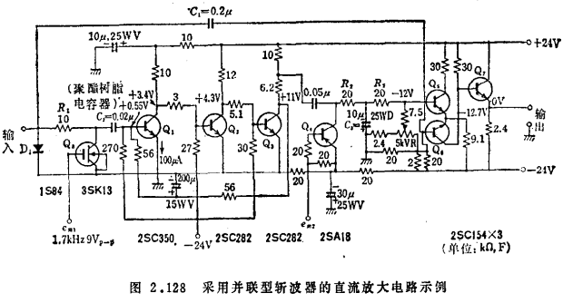
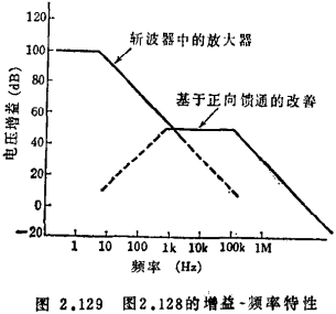
Figure 2.128 is an example of using a parallel chopper. Here, the DC coupling circuit composed of Q5~Q7 is connected behind the synchronous detection, the output resistance is reduced to 0.5kQ, and the maximum output voltage is improved to more than 10V at the same time. The DC gain of the whole circuit is 100dB. MOS transistor chopper amplifier circuit. The diode D1 connected to the input terminal is used to protect the maximum input voltage. In addition, the frequency bandwidth of the chopper amplifier circuit itself is mainly restricted by the low-pass filter (R2, R3, C3) behind the synchronous detection. This point can be used to connect the input terminal to the coupling capacitor of the base of Q6, which is called The coupling method of the forward feedthrough method is improved, and the high frequency end of the frequency band is improved (see Figure 2.129).

Figure 2.130 is the design of the compound DC amplifier circuit for measuring the weak current of 10-10~10-12A. In order to improve the input impedance of the two AC amplifying circuits, junction field effect transistors are used in the primary stage, and HA1303M bipolar integrated circuit operational amplifiers are used in the secondary stage. Table 2.16 lists the performance of the composite DC amplifier circuit. The offset current is the sum of the pumping current and the peak current of the chopper, with a value below 10-9A; the changing part of the offset current shows a current drift, with a value below 2×10-12A/℃. Therefore, if the offset current is compensated at the input, a weak current of about 2×10-12A can be stably detected. MOS transistor chopper amplifier circuit. As described in section 2.2.4, in order to detect weak currents, a DC-coupled amplifier circuit composed of MOS field effect transistors can be used. However, in order to avoid voltage drift during startup and over time, and to improve detection sensitivity, the detection resistance must be increased. For the detection sensitivity of 1×10-12A, the negative feedback resistance R should be above 1×10¹⁰Ω. On the other hand, since the frequency bandwidth becomes narrower proportionally as Rf increases, Rf must be lowered in order to achieve a wider frequency band. The circuit in Figure 2.130 reduces Rf to 1×10⁹ for this purpose to maximize the performance of the MOS transistor chopper.
Contact: Mr. Zou
Contact number: 0755-83888366-8022
Mobile phone: 18123972950
QQ: 2880195519
Contact Address: 5C1, Block CD, Tianji Building, Tianan Digital City, Chegongmiao, Futian District, Shenzhen
Please search WeChat official account: "KIA Semiconductor" or scan the following picture to "Follow" official WeChat official account
Please "follow" the official WeChat account: provide MOS tube technical assistance


