Electronic Technology Forum
There are two kinds of current analysis details for the constant current deviation of MOS transistors
The constant current offset of the MOS transistor chopper can be divided into the following two types.
1) Peak current (electrostatic induction current of the driving voltage source through the capacitance between the electrodes)
2) Pumping current
The above two components are directly proportional to the driving frequency. In this regard, they are similar, but their polarities cancel each other out; in addition, the relationship with the driving voltage is also different, so they cannot be discussed as one category.
Now take the parallel chopper circuit as an example, try to find the size of the spike. Figure 2.117 shows the parallel chopper circuit, and the equivalent circuit is as shown in Figure (b). The square wave drive voltage is differentiated by the inter-electrode capacitance CGD, and its output voltage on the drain side is shown in Figure (C), showing a pulse waveform that decays according to an exponential function. The constant current of the MOS transistor shifts. The time constant of the spike generated when the chopper is switched from on to off is very large, and the time constant from off to on is very small, so the area of the two spikes is the integral value of time , The former is much larger than the latter. The former is called the area of the turn-off peak, and the latter is called the area of the turn-on peak. These spikes are amplified by the AC amplifier and converted into DC by the synchronous detection circuit (including the low-pass filter after the detection). On the other hand, the DC input signal is also demodulated into DC after being converted into a square wave by the chopper. Therefore, the magnitude of the DC offset caused by the spike must be obtained by dividing the synchronous detection output signal by the DC gain. The detection efficiency of the synchronous detection circuit depends on different circuit structures, and the peak and square wave signals are often different. Therefore, only the peak waveform generated in the input circuit of the chopper is known, and it is impossible to obtain the converted value of the DC offset. The constant current of the MOS transistor shifts. Therefore, in general, the synchronous detection circuit is idealized. For spikes and square wave signals, the average value in one period is taken as the converted value of DC offset. This method can get roughly correct results for many synchronous detection circuits.
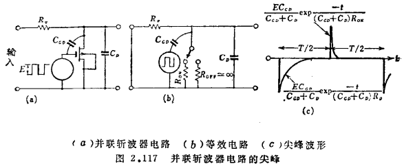
It can be seen from Figure 2.117(C) that the turn-off spike in the parallel chopper circuit is proportional to the resistance of the signal source, and the turn-on spike is proportional to the on-resistance of the chopper, so the area of the turn-off spike is larger, and its DC The offset conversion value is as follows.
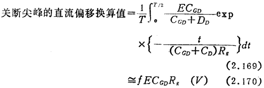
It is proportional to driving frequency f, driving voltage amplitude E, inter-electrode capacitance CGD and signal source resistance Rg. Since the spike pulse is proportional to Rg, it is a constant current offset source. f. Rg cannot be reduced arbitrarily due to circuit performance. When MOS field effect transistors are used as choppers, they must compensate for the work from on to off, and E cannot be reduced below the necessary amplitude, so in order to reduce this offset , Other capacitors should be added to offset the impact of CGD.
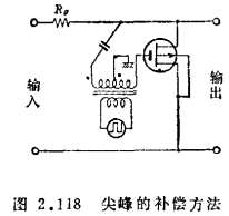
To this end, one method uses the reverse phase power supply shown in Figure 2.118, and the other method adds a MOS-type field effect transistor. A typical example of the latter method is a series-parallel chopper circuit.
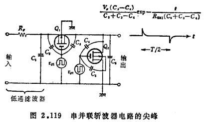
In the series-parallel chopper circuit shown in Figure 2.119, the inter-electrode capacitance of the MOS field effect transistor is set as C2, C2, C4, C5, Rg, and C1 to form a low-pass filter. The capacitance C1 is compared with the above-mentioned inter-electrode capacitance It is much larger, so the spike current flowing through C2 is grounded through C1, and its influence will not appear at the output. Similarly, the spike current flowing through C5 can also be ignored. The constant current of the MOS transistor shifts. Therefore, the spike voltage appearing at the output is generated by C3 and C4. Since the two MOS field effect transistors work in opposite phases, the phases of υg1 and υg2 are just opposite. Assuming that the two have the same amplitude E, the output peak voltage waveform is

Its DC offset conversion value is●)

Explanation: ●) According to the same discussion method as formulas (2.169) and (2.170), since formula (2.172) is the average value of formula (2.171) in a period, it should be equal to fE(C3-C4)Ron. However, if we observe the operation of the series-parallel circuit in detail, we can see that the spike generated at the moment when Q1 is switched from off to on state is first charged to C6, and then discharged by Ron and Rg of Q1, so it should be the formula (2.172). On the contrary, the spike generated at the moment when Q1 is switched from on to off state is first charged to C6 and then discharged by Ron of Q2, so it can be ignored compared with equation (2.172).
Comparing equation (2.170) and equation (2.172), it can be seen that CGD is compensated by (C3-C4). Therefore, in order to effectively reduce the peak offset in the series-parallel circuit, components with equal capacitance between electrodes should be used as much as possible. MOS integrated circuit components are very suitable. The inter-electrode capacitance of commercially available MOS field effect transistors, including the capacitance of the sealed case, is approximately (see Figure 2.120)
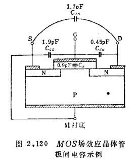
CGD、C1、C2等 0.5pF (2.173)
Therefore, if Rg=100kΩ, f=1kHz, E=5V, the peak offset Vo of the parallel chopper circuit can be obtained by equation (2.170)


However, the capacitance deviation between the electrodes of the series-parallel circuit using MOS integrated circuits is less than 5%, so

It can be improved by more than one order of magnitude.
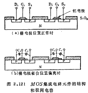
Figure 2.121(a) is a schematic diagram of a cross-section of an integrated circuit element containing two MOS field effect transistors. In the process flow of this integrated circuit element, if the nesting position of the gate electrode mask is deviated, the gate electrode is as shown in Figure (b), although ,
,
But there are big differences between C2 and C5 and C3 and C4. In order to prevent the increase of spikes caused by the unevenness of the process, the serial numbers of the capacitors in Figure 2.121 should be wired corresponding to the serial numbers of the capacitors in Figure 2.119.
The offset voltage caused by the spike signal in the series-parallel chopper circuit depends on the deviation of the inter-electrode voltage C3 and C4 according to the relationship of formula (2.172). Therefore, when using MOS transistors of the same type, this offset voltage must have a random deviation centered on zero. However, in fact, when using P-channel enhancement mode MOS transistors, the polarity of the offset voltage is always negative; when using N-channel depletion mode MOS transistors, the polarity of the offset voltage is always positive (C1 terminal in Figure 2.119). Voltage). The constant current of the MOS transistor shifts. This tells us that there are other reasons for the offset voltage source of the MOS crystal chopper in addition to the spike signal and the thermoelectromotive force. The reason for this is the offset current 61) 62) based on the pumping operation cited at the beginning of this section.
As shown in the inset in Figure 2.122, the source, drain and silicon substrate of the P-channel MOS field effect transistor are respectively connected to a DC current meter. When the same driving voltage as the chopper is applied to the gate, there is a DC current Flow through each ammeter in the direction shown in the figure. The magnitude of the current, as shown in Figure 2.122, is proportional to the frequency and almost independent of the resistance R, and the sum of the source and drain currents is equal to the silicon substrate current. Therefore, a direct current flows from the source and drain to the silicon substrate.
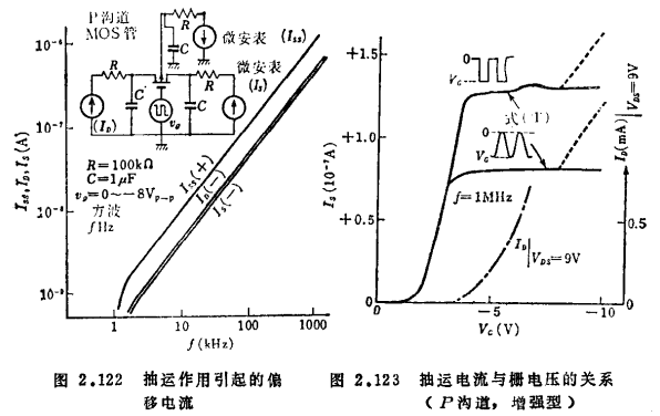
Since there is no DC electromotive force in this loop, it can be considered that the cause of the DC current is the AC charge generated by the gate electrode in the channel through electrostatic induction, which is rectified and distributed to the electrodes in the channel. Figure 2.123, Figure 2.124, and Figure 2.125 are examples of the relationship between the offset current and the gate voltage. When using a voltage drive from zero to -VG, in a P-channel device, as can be seen from Figure 2.123, when VG exceeds the pinch-off voltage Vp, the pumping current tends to be approximately a constant saturation value. In addition, in N-channel devices, the pumping current surges when VG exceeds Vp. Therefore, from the viewpoint of reducing the drift caused by the change in the driving voltage, the P-channel enhancement type device is better.
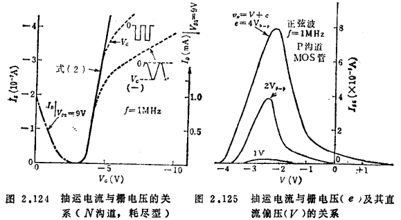
Figure 2.125 shows that when the driving voltage and the DC bias are superimposed, the offset current is at its maximum near Vp under the same DC bias. In order to ensure the on-off action of the chopper, it should be driven around the pinch-off voltage. Comparing Figure 2.125 with Figure 2.123 and Figure 2.124, it can be seen that in order to reduce the offset current, it is advisable to drive with the smallest possible amplitude near Vp.
Here is an example for reference: Set Rg=100kΩ, f=1kHz, Vg=0~-5V, as can be seen from Figure 2.123, the offset voltage at the input end is 13μV. Compared with the peak offset of formula (2.175), this value is roughly the same magnitude; if MOS integrated circuit elements with small capacitance deviation between electrodes are further used, this value becomes a decisive component.
Contact: Mr. Zou
Contact number: 0755-83888366-8022
Mobile phone: 18123972950
QQ: 2880195519
Contact Address: 5C1, Block CD, Tianji Building, Tianan Digital City, Chegongmiao, Futian District, Shenzhen
Please search WeChat official account: "KIA Semiconductor" or scan the following picture to "Follow" official WeChat official account
Please "follow" the official WeChat account: provide MOS tube technical assistance


