Electronic Technology Forum
Overview of MOS Field Effect Transistor Modulated DC Amplifier Circuit and Characteristics
The modulated DC amplifier circuit is a circuit that converts DC and low-frequency signals into high-frequency AC signals through a DC-AC converter, and then demodulates them by a synchronous detection circuit after amplification. Because the AC amplifier prevents the DC component from passing, no drift occurs. Therefore, if a low-drift DC-AC converter can be obtained, a more stable DC amplification can be achieved than the DC-coupled amplifiers in the above sections. MOS tube modulation type DC amplifier circuit. There have been many types of DC-AC converters in the past, which are roughly divided into chopper type and parametric amplifier type. The chopper type uses switching elements to convert DC signals into on-off AC, and MOS field-effect transistors are also included in this category.
The components of the chopper are required to have the following four important characteristics.
1) High DC-AC conversion efficiency.
2) Good linearity.
3) Easy to drive, stable characteristics for a long time.
4) The offset and drift are almost low.
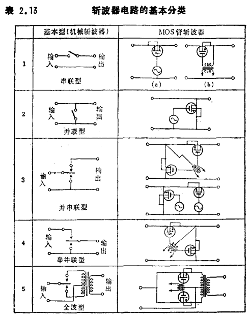
The chopper circuit can basically be divided into five types as shown in Table 2.13. Recently, because integrated circuit-type components are not difficult to obtain, there is no need to save the number of switching components, so 4) series-parallel type and 5) full-wave type are often used. Series-parallel type, high input impedance, high DC-AC conversion efficiency, and has the effect of compensating spikes (described later). The full-wave mode transforms the frequency of the input signal that is the same as the modulation frequency into twice the frequency component. MOS tube modulation type DC amplifier circuit. Therefore, if the mains frequency is used for modulation, the induced noise component entering the input terminal is transformed into a component of twice the frequency, and then it can be filtered out by the filter in the AC amplifier circuit.

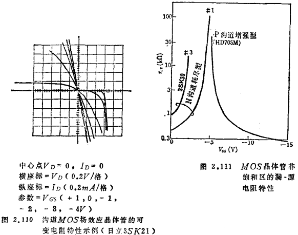
Figure 2.110 shows the VD-ID characteristics of an N-channel MOS transistor near the origin. In the second quadrant of the graph, in The sharp increase in ID is due to the positive P-N junction between the P-type silicon substrate and the N-type drain. Therefore, unless special measures are taken, the input voltage range that can be applied to the MOS transistor switch is only below 0.6V. The internal resistance rd can be given by the slope near the origin. MOS tube modulation type DC amplifier circuit. Figure 2.111 is an example of the relationship between rd and VGS. When using a MOS transistor as a switching element, it is necessary to transition from a low-resistance state to a high-resistance state by applying VGS stepwise. The size of rd near the origin, theoretically


This formula shows that the internal conductance (1/rd) of the MOS transistor is roughly linearly controlled by VGS, which means that in addition to being used as a switch, it can also be used as a variable resistance element (attenuator, etc.), and its application range is very wide. .
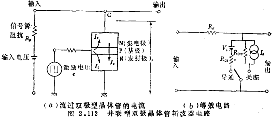
Compared with other semiconductor choppers, the biggest advantage of MOS transistor choppers is that their offset and drift levels are particularly low. This can be understood by comparing with the original bipolar transistor chopper. Figure 2.112 (a) is a parallel chopper circuit using bipolar transistors. In the on state, both P-N junctions are driven in the forward direction, so I1 and I2 are the currents flowing through the P-N junctions, and I3 is the current that flows through the transistors formed by I1 and I2. Because these currents produce forward voltage drops on the two P-N junctions, the polarities of the two forward voltage drops exactly cancel each other, and the voltage difference is the voltage offset Vo. In the off state, a saturation current flows in the two reverse-biased P-N junctions, resulting in a current offset Io. Figure 2.112 (b) is the equivalent circuit representation of Vo and Io. Vo and Io correspond to the voltage offset and current offset of the DC coupling amplifier circuit in the previous section. Therefore, their change is drift, which gives the upper limit of the sensitivity of DC amplification. It can be seen from the above description that the root cause of Vo and Io is the fact that the current flows from the base power supply (drive power) into the transistor. MOS tube modulation type DC amplifier circuit. The driving voltage of the MOS transistor is applied through a high-quality insulator-silicon dioxide, so the current flowing in from the driving source can be completely ignored. Therefore, there is no offset equivalent to Vo and Io, and as a chopper element, it can achieve unprecedented high sensitivity. In addition, since there is no offset source, there is no need for various offset compensation circuits, and the circuit structure is simple.

The above is the reason why the MOS transistor can be used as the main chopper element in the future.
However, all DC-AC converters have some common problems, that is, the thermoelectromotive force that inevitably occurs between the signal wire material (mainly copper or galvanized copper wire) and the material used as the chopper To cause drift, the electrostatic induction of the driving voltage source through the inter-electrode capacitance will produce an offset (spike signal), and the drift caused by these changes.
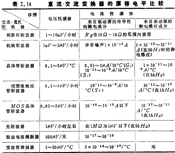
Table 2.14 compares the drift levels of the prepared DC-AC converters. The mechanical chopper has the longest history and is a product that has reached the limit in terms of performance. The best product has a sensitivity of 1nV (1×10⁻⁹V). The semiconductor chopper is inferior to the mechanical chopper from the perspective of drift, but it far exceeds the mechanical chopper in terms of broadband and reliability (lifetime). The voltage drift of the captive tube chopper shown here is a value when the aforementioned Vo is minimized by appropriately adjusting the driving conditions, and a circuit structure that compensates for the drift is adopted at the same time. Compared with transistor choppers, junction and MOS field effect transistor choppers do not need to take such measures. However, it is actually very difficult to make the drift level as low as 0.05μV/hour or less, because it is related to the measures taken to overcome the aforementioned thermoelectromotive force. The constant current offset is roughly divided into the conductive leakage component from the driving source and the electrostatic induction component through the inter-electrode capacitance. The latter increases in proportion to the drive frequency, and the value given in the table is at 1kHz.

Contact: Mr. Zou
Contact number: 0755-83888366-8022
Mobile phone: 18123972950
QQ: 2880195519
Contact Address: 5C1, Block CD, Tianji Building, Tianan Digital City, Chegongmiao, Futian District, Shenzhen
Please search WeChat official account: "KIA Semiconductor" or scan the following picture to "Follow" official WeChat official account
Please "follow" the official WeChat account: provide MOS tube technical assistance


