Electronic Technology Forum


Detailed explanation of the switched capacitor multivibrator circuit and its waveform analysis
The switched capacitor circuit can also be used to design a switched capacitor multivibrator. The circuit is shown in Figure 6.1-5a. Op amps A1, A2 and capacitor a1C form a positive feedback loop, A1 is an integrator, and A2 is a comparator. If the comparator output voltage Vo is limited to the negative power supply Vss, the switched capacitor a2C feeds positive charge to the integrating capacitor C in each clock cycle ,In this way, the output voltage V1 of the op amp A1 is correspondingly reduced by the step voltage a2lVssl (see Figure 6.1-5b). If it drops to V1<0, then
 the comparator output voltage Vo jumps to the positive power supply VDD, at this time, the coupling capacitor a1C feeds positive charge to the integrating capacitor C
 ,Make V1 jump down to a1 (VDD-VSS). In each clock cycle thereafter, a2C feeds the negative charge-a2VDD to the integrating capacitor C, so that V1 generates a positive step a2VDD. If it rises to V1>0, Vo jumps to the negative power supply Vss. The above process continues to repeat.
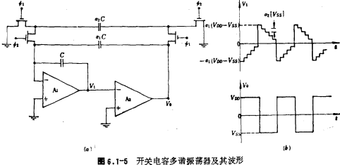
If a2< a1, Vss=-VDD, the oscillation must rate of this circuit is

Where fcx is the clock frequency.
From the equation (6.1-7), we can see that the circuit in Figure 6.1-5a can be used as a frequency divider circuit.
Contact: Mr. Zou
Contact number: 0755-83888366-8022
Mobile phone: 18123972950
QQ: 2880195519
Contact Address: 5C1, Block CD, Tianji Building, Tianan Digital City, Chegongmiao, Futian District, Shenzhen
Please search WeChat official account: "KIA Semiconductor" or scan the following picture to "Follow" official WeChat official account
Please "follow" the official WeChat account: provide MOS tube technical assistance

