Electronic Technology Forum
Analysis of Biquad Transfer Function and Circuit Structure of Switched Capacitor Filter
Double second-order switched capacitor filter
Earlier we discussed the use of passive RLC networks to design switched capacitor filters. This design method is mainly used for low-pass and band-pass designs. It is more difficult to design high pass or band stop. Even if it is designed, the circuit structure is often complicated and the capacitor area is large, so it is rarely used. Below we introduce a double second-order switched capacitor filter structure. Using the double second-order switched capacitor filter circuit can easily design various filters such as low-pass, high-pass, band-pass and band-stop, and connect this circuit in series to realize a high-order filter. However, the high-order or high-Q switched capacitor filter realized by this method has high sensitivity, so its practicability is reduced.
1. Double second-order transfer function
It can be seen from the second section of this chapter that any high-order transfer function in the S-domain can be decomposed into the form of first-order and second-order multiplication. Among the second-order transfer functions: the representative is the double-second-order transfer function, which represents

Using the above formula, various filters such as second-order low-pass (b2=b1=0), high-pass (b2=bo=0), band-pass (b1=0), and band-stop can be realized. The switched capacitor filter realized by the biquad transfer function is called the biquad switched capacitor filter. For the convenience of discussion, the formula (5.3-29) can also be written as

In the formula, ωP is the frequency of the pole, and Q is the Q value of the pole corresponding to the pole. From the equations (5.3-29) and (5.3-30), the following relationship can be obtained:

2. Circuit structure of double second-order switched capacitor filter
In order to obtain the block diagram of the biquad transfer function H(S), formula (5.3-30) is rewritten as

Divide both sides of the above formula by S2, and get


V1 in the formula is expressed as

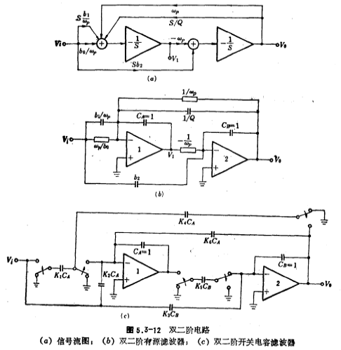
From equations (5.3-33) and (5.3-34), the signal flow diagram shown in Figure 5.3-12a can be drawn, which contains two inverting integrators to generate -1/S operation. If the inverting integrator is realized by an operational amplifier with a feedback capacitor C=1, then the transmission branches ωP, bo/ωP and -ωP become the integral resistance of the inverting integrator, and their values are 1/ωP, ωP/ bo and -ωP; and the transmission branches S/Q, Sb1/ωP and b2S respectively become inverting integrators, and the input capacitors 1/Q, b1/ωP and b2 constitute an addition circuit. Therefore, the signal flow diagram shown in Figure 5.3-12a can be realized by a dual second-order active RC circuit, and its circuit form is shown in Figure 5.3-12b. If the positive resistance in the figure is replaced by the switched capacitor circuit in Figure 5.3-2b, and the negative resistance is replaced by the switched capacitor circuit in Figure 5.3-2c, then a double second-order switched capacitor filter can be obtained. The circuit is shown in Figure 5.3- Shown in 12c. According to the formula (5.3-3), the capacitance value of the switched capacitor is C=T/ (
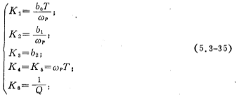
( is the equivalent analog resistance), then the capacitance values in the figure are

The pole angle rate ωP is approximately equal to the filter cut-off angle frequency ωc. To make the equation (5.3-35) hold, it should satisfy
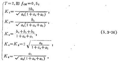
 .According to the formulas (5.3-35) and (5.3-30), we can design double second-order low-pass, high-pass, band-pass and band-stop switched capacitor filters, but this design method is not accurate. If you want to design accurately, you can use the following design formula:

In the formula, ao, a1, bo, b1 and b2 are the coefficients of (5.3-29). The switching clock signal cycle T=2 is just for the convenience of calculation, it is only a relative value.
[Example 15] Design a second-order band-pass switched capacitor filter, the main parameters: (1) The center frequency of the pass band is fo, the corresponding gain Ao=10; (2) Q=70; (3) The switching clock signal must rate The ratio of fcx to the passband center frequency fo is 20.
Solution i. Use the circuit form shown in Figure 5.3-12c.
ii. Calculate the coefficients of the biquad function:
The bandpass transfer function is

From the formula (5.3-36), fcx=0.5, fcx/fo=20 is used, so the bandpass center frequency fo=0.025 and ωo=0.157.
and

iii. Calculate the capacitance value in the figure:
It can be obtained by (5.3-36)

iv. Take the capacitance value:
In order to obtain a smaller capacitance area, the and
and as a group,
 and
and for another group, take the smallest capacitance value in the group as 1 unit capacitance, in
 the capacitance is the smallest, so the capacitance value in this group is

Another group of capacitors,  has the smallest capacitance, so take

In this example, if the center frequency fo of the passband is taken as fo=1, then the required clock frequency fcx=20 kHz.
[Example 16] Using the double second-order switched capacitor filter shown in Figure 5.3-12c, design a fourth-order Chebyshev high-pass switched capacitor filter with a passband fluctuation of 0.25 decibels, and take fcx/fc=200.
Solution i. Calculate the transfer function of the Chebylev low-pass filter with a normalized fourth-order and passband fluctuation of 0.25 dB:
Its transfer function is

The parameters provided in Table 5.1-4 are obtained after conversion

and

ii. Calculate the high pass transfer function
After frequency conversion of the low-pass transfer function, that is, in the formula (5.3-37), S is replaced by ωc/S, and the high-pass transfer function can be obtained:

The fourth-order high-pass filter is realized by connecting two double second-order switched capacitor filters (Figure 5.3-12c) in series. Now calculate the capacitance values in the first-stage and second-stage double second-order high-pass switching electric filter.
iii. Calculate the capacitance value in the first-stage double second-order high-pass switched capacitor filter:
(5.3-38) The coefficients a1, a2 and b2 in the formula are

By (5.3-36) the capacitance value is

take unit capacitance,

iv. Calculate the capacitance value in the second-stage double second-order high-pass switched capacitor filter:

take unit capacitance,

In this example, if the clock signal frequency fcx=200 kHz, then the cut-off frequency of the high-pass filter fc=1 dry Hz.
It can be seen from the above two design examples that the transfer function H(S) of the filter in the S domain is first obtained, and then the formula (5.3-36) is used to calculate each of the two second-order switched capacitor filters in Fig. 5.3-12c The capacitance value of the capacitor. In this way, it is easier to design various types of switched capacitor filters.
Contact: Mr. Zou
Contact number: 0755-83888366-8022
Mobile phone: 18123972950
QQ: 2880195519
Contact Address: 5C1, Block CD, Tianji Building, Tianan Digital City, Chegongmiao, Futian District, Shenzhen
Please search WeChat official account: "KIA Semiconductor" or scan the following picture to "Follow" official WeChat official account
Please "follow" the official WeChat account: provide MOS tube technical assistance


