Electronic Technology Forum
Common filter low-pass, high-pass, band-pass design methods and basic detailed explanations
Simulation Method of RLC Ladder Network
1. Low-pass filter
(1) Design of third-order low-pass filter
We take the design of a third-order low-pass switched capacitor filter as an example to illustrate the design method and steps of a low-pass switched capacitor filter. The third-order passive RLC ladder-type filter is shown in Figure 5.3-7a, and its node voltage and branch current are described by the following equations
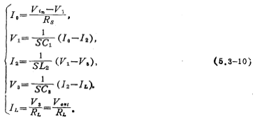
In order to change the current quantity of the above formula to the voltage quantity, a proportional resistor R is introduced, and  (i is the footnote of the current I of the above formula). The above formula is written as
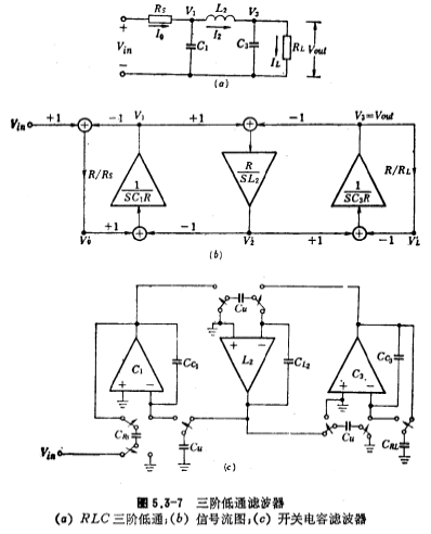
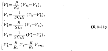
From equation (5.3-11), the signal flow diagram shown in Figure 5.3-7b can be obtained. There are three integrators in the figure, and their time constants are respectively C1R, L2/R and C2R. After finishing (5.3-11) formula, the following formula can be obtained

According to the signal flow diagram shown in Figure 5.3-7b and equation (5.3-12) and the conversion relationship between the RC integrator and the switched capacitor integrator (Figure 5.3-4), the third-order shown in Figure 5.3-7c can be obtained Low-pass switched capacitor filter. The switch capacitor integrator at all levels in the figure is the circuit shown in Figure 5.3-4. For simplicity, the switch is drawn in another form. Low pass, high pass, band pass. If the integration time constant of the switch capacitor integrator at each level of the circuit corresponds to and equals the integration time constant in the equation (5.3-12), the following equation can be obtained: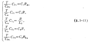
After finishing the above formula, we get
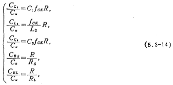
Where fcx is the clock signal frequency when normalized (ωc=1 radians/sec). Under normal conditions, take Rs=RL=R=1 ohm, then (5.3-14) formula is written as
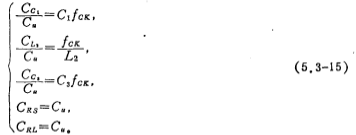
From equation (5.3-14) or (5.3-15), as long as you know the inductance L, capacitance C, input resistance Rs and terminal resistance RL of the RLC ladder filter under normalized conditions, and the normalized With the clock signal frequency fcx, the capacitance ratio of each switched capacitor integrator in the circuit of Figure 5.3-7 (c) can be obtained. Low pass, high pass, band pass. In order to make the characteristics of the switched capacitor filter close to the characteristics of the RLC filter, the actual clock signal f'cx should be much larger than the cut-off frequency fc of the low-pass filter, and the relationship is

Under normalized conditions, ωc=1 radian/second, so the normalized clock signal frequency fcx has the following relationship:

For a low-pass filter, generally  takes 20-40. If
  is too large, increase the capacitance ratio of the integrator and increase the chip area.
Figure 5.3-7a The parameters of the RLC ladder filter can be found in Table 5.3-1. For the normalized (Rs=RL=1 ohm, ωc=1 radians/sec) third-order Butterworth low-pass filter, the specific parameters are

If the ratio of the clock signal frequency f'cx and the cutoff frequency fc of the low-pass filter is taken as  , the equations (5.3-17) and (5.3-15) can be used to obtain the switch capacitor integrator in Figure 5.3-7c The capacitance ratio, namely
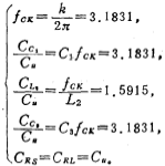
If take unit capacitance, then
 unit capacitance,
 unit capacitance,
 unit capacitance,
 unit capacitance,
Obviously, the unit capacitance the smaller the value, the smaller the total capacitance value of the switched capacitor filter. However, the size of the unit capacitance is restricted by the size of the parasitic capacitance.
 Pifa.
Pifa.
All of the above calculations are carried out under normalized conditions. If you want to change the frequency of the low-pass cut-off angle frequency ωc, you only need to calculate the actual clock color rate according to the value of ωc and use the formula (5.3-16) , And no correction is made to the capacitance ratio obtained by normalization. Low pass, high pass, band pass. The calculation step is to first calculate the capacitance ratio from equations (5.3-17) and (5.3-15) under normalized conditions, and then calculate the actual required clock frequency f'cx according to the required cut-off frequency fc. If the cut-off frequency of the third-order low-pass filter in the above example is fc=1, the actual clock rate can be obtained by formula (5.3-16)
 kilohertz.
From the above discussion, it can be seen that for the switched capacitor filter, the clock frequency is determined And filter cutoff frequency fc
After the ratio of image.png, adjust the clock frequency , You can change the cutoff frequency fc of the filter according to the scale factor of
  the design method of the third-order low-pass switched capacitor filter is discussed above.
Undoubtedly, using similar design steps, high-order all-pole low-pass switched capacitor filters can be designed. The design method of the elliptic function low-pass filter is discussed below.
(2) Design of elliptic function low-pass switched capacitor filter
The elliptic function low-pass switched capacitor filter is realized by a passive RLC elliptic function low-pass filter through transformation.
Now take the fifth-order elliptic function low-pass switched capacitor filter commonly used in communication systems as an example to illustrate its design method. Figure 5.3-8 is a fifth-order RLC elliptic function low-pass filter, and its normalized component values can be found in Table 5.3-3. Low pass, high pass, band pass. From Figure 5.3-8, the following voltage and current equations can be obtained:
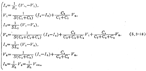
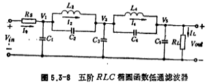
In order to change the current quantity into the voltage quantity in the above formula, a proportional resistor R is introduced, so that ,thus, (5.3-18) can be written as
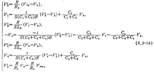
It can be seen from the above formula that the relationship between the voltages can be realized by an integrator and an adder. In order to facilitate the selection of a switched capacitor integrator with an adder, V3 in the formula is rewritten as -V3.
The signal flow diagram drawn according to equation (5.3-19) is shown in Figure 5.3-9a. In the figure, the integration time constants of integrators 1, 2, 3, 4 and 5 are respectively (C1+C2) R, L2/R, (C2+C3+C4) R, L4/R and (C4+C5) R, The values of a are expressed as follows:
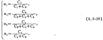
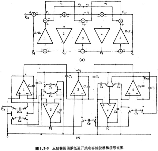
(5.3-19) The proportional resistance R in the formula can usually be selected according to the maximum dynamic range of the filter and the smallest capacitance area (refer to this section 4). For simplicity, take R=1 ohm. Low pass, high pass, band pass. The normalized resistance Rs and RL in Figure 5.3-8 are usually 1 ohm, so Rs=RL=R=1 ohm, according to the signal flow diagram shown in Figure 5.3-9a and Rs=RL=R=1 Ohm condition, the fifth-order elliptic function low-pass switched capacitor filter shown in Figure 5.3-9b can be obtained, which corresponds to the integration time constant of Figure 5.3-90.b, and equals it. According to equation (5.3-19), we can find Obtain the capacitance value of each integrator in Figure (b), and its value is expressed by the following formula
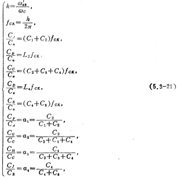
Where ω'ck is the actual clock angle whisker rate, ωc is the cut-off angle frequency of the filter, and fcx is the clock frequency when the cut-off angle frequency of the filter is 1 radian/sec. In order to make the passband gain 0 dB, the input capacitance is from ,expanded to
 。
。
[Example 12] Design a fifth-order elliptic function low-pass switched capacitor filter, the main parameters: (1) passband fluctuation RP=0.1dB; (2) stopband minimum attenuation decibels; (3) Stopband angular frequency Ωs=1.20 radians/sec when normalized; (4) Cutoff frequency fc=3.4 kHz; (5) Clock signal frequency
 = 128 kHz.
Solution i. Determine the value of each component in the circuit of Figure 5.3-8:
Look up Table 5.3-3 to get
Rs=RL=1 ohm, C1==0.91441, C2=0.31628, L2=1.06516, C2=1.38201, L4=0.60131, C4=1.09329, C5=0.52974.
ii. Calculate the ratio of the clock frequency f'ck and the cutoff frequency fc image.png:

iii. Calculate the normalized clock frequency fcx:

iv. Calculate the capacitance ratio:
According to (5.3-21) formula

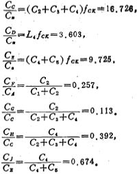
v. Calculate the value of each capacitance:
take unit capacitance; CA=7.374 unit capacitance; CB=6.382 unit capacitance; Cc=16.726 unit capacitance; CD=3.603 unit capacitance; CE=9.725 unit capacitance; CF=1.895 unit capacitance; CG=1.890 unit capacitance; CE =6.557 unit capacitance; CJ=6.555 unit capacitance.
2. Band pass filter
The design steps of the band-pass switched capacitor filter: firstly, the RLC low-pass filter is converted through frequency to obtain the RLC band-pass filter; secondly, the equations of the voltage and current of each node, branch of the RLC band-pass filter are listed, and then Draw a signal flow diagram according to the voltage and current equations: Finally, the band-pass switched capacitor filter is obtained from the signal flow diagram.
The RLC second-order normalized low-pass filter is shown in Figure 5.3-10a. Low pass, high pass, band pass. According to the frequency conversion relationship from low-pass to band-pass, Figure 5.3-10a is transformed into the RLC band-pass filter shown in Figure 5.3-10b. Its component value is

Where C1 and L2 are the RLC second-order normalized low-pass filter component values, ωo is the center corner frequency of the band-pass filter, and B is the band-pass filter's 3 decibel bandwidth.
From Figure 5.3-10b, the following voltage and current equations can be obtained:
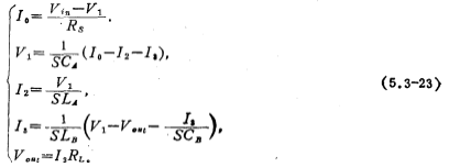
Use proportional resistance R to change the amount of current in the above formula to voltage and express it with t, then the above formula can be rewritten as
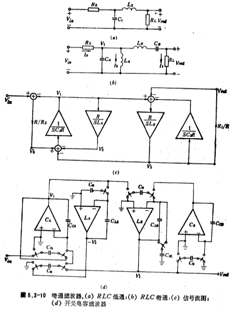
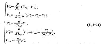
Draw the signal flow diagram as shown in Figure 5.3-10c according to formula (5.3-24), from which the band-pass switched capacitor filter circuit can be obtained, and its circuit form is shown in Figure 5.3-10d. For simplicity, take Rs=RL=R=1 ohm, so CRs, CRL and the same i.e.
 。.The capacitance ratio of each switched-capacitor integrator in the figure is obtained by (5.3-25) equation, which is expressed as
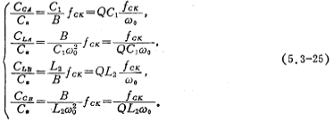
Where Q is the Q value of the band-pass filter.
[Example 13] Design a fourth-order Butterworth switched capacitor filter, its clock signal frequency fcx is 20 times the band-pass center frequency fo, and the band-pass Q value is 5.
Solution i. Calculate the component values of Figure 5.3-10a:
From Table 5.3-1
Rs=RL=1 ohm, C1=1.4142, L2=1.4142
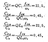
ii. Calculate the capacitance ratio of each switched capacitor integrator in Figure 5.3-10d:
From the equation (5.3-25), the capacitance ratio of each integrator is as follows:
3. High-pass filter
The design steps of the high-pass switched capacitor filter are: (1) The RLC high-pass filter is obtained after frequency conversion by the RLC low-pass filter; (2) The voltage and current equations of each node and branch of the RLC high-pass filter are listed: ( 3) Draw a signal flow diagram according to the voltage and current equations; (4) Draw a high-pass switched capacitor filter from the signal flow diagram. Figure 5.3-11a shows the RLC fourth-order high-pass filter, which is directly obtained by transforming the RLC low-pass filter. Just replace L in the low-pass filter with C and C with L, and the component values between them Reciprocal of each other.
From Figure 5.3-11a, the following voltage and current equations can be obtained:
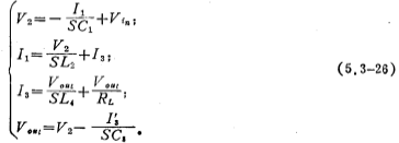
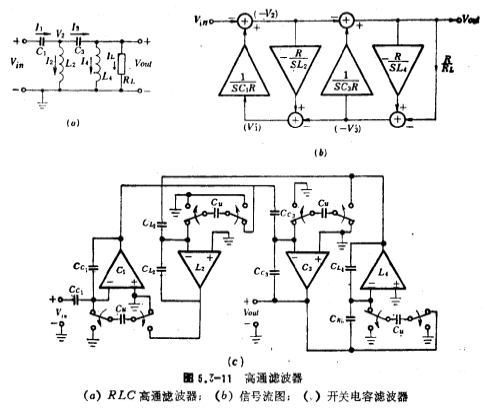
Introduce the proportional resistance R to change the amount of current in the above formula to the amount of voltage, and the relational formula is , So the above formula can be written as
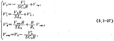
From the formula (5.3-27), draw the signal flow diagram as shown in Figure 5.3-11b. According to this signal flow diagram, a fourth-order high-pass switched capacitor filter is obtained, and its circuit form is shown in Figure 5.3-11c. Low pass, high pass, band pass. For simplicity, take RL=R=1 ohm. The capacitance ratio of the circuit is obtained by the following formula
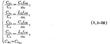
Where ωc is the cut-off frequency of the high-pass filter.
[Example 14] Design a fourth-order Butterworth high-pass switched capacitor filter, the ratio of the clock frequency fcx to the cut-off frequency fc is 100.
Solution i. Calculate the parameters of the normalized fourth-order Butterworth low-pass filter:
From Table 5.2-3
RL=1 ohm, L1=1.5307, C2=1, 5772, L3=1.0824, C4=0, 3827
ii. Calculate the parameters of the normalized fourth-order Butterworth high-pass filter:
According to the conversion relationship between the low-pass filter and the high-pass filter, the inductance and capacitance values in the high-pass filter are obtained

iii. Calculate the capacitance ratio of 5.3-11 (c) circuit:
From the formula (5.3-28)

Contact: Mr. Zou
Contact number: 0755-83888366-8022
Mobile phone: 18123972950
QQ: 2880195519
Contact Address: 5C1, Block CD, Tianji Building, Tianan Digital City, Chegongmiao, Futian District, Shenzhen
Please search WeChat official account: "KIA Semiconductor" or scan the following picture to "Follow" official WeChat official account
Please "follow" the official WeChat account: provide MOS tube technical assistance


