Electronic Technology Forum
The Basic Working Principle and Design Method Analysis of Switched Capacitor Filter
Switched capacitor filter
Switched capacitor filter is a novel integrated filter made up of basic components such as MOS operational amplifier, switch and capacitor, and made by MOS integrated circuit technology. In addition to the advantages of small size, low power consumption, and convenient debugging, it also has the following characteristics:
1. The time constant of the switched capacitor filter is determined by the ratio of the two capacitors, and has nothing to do with the absolute value of the capacitor. In the MOS integrated process, the relative error of the capacitor ratio is less than 1%, and it has a low temperature coefficient. Therefore, the switched capacitor filter has excellent stable performance.
2. The switched capacitor filter works under the action of a clock signal. Changing the frequency of the clock signal can easily adjust the frequency characteristics of the filter without adjusting the component values in the circuit.
3. Because the MOS digital circuit of the MOS digital circuit is compatible with the MOS process of the switched capacitor filter, the digital circuit and the switched capacitor filter and other analog integrated circuits can be integrated on the same chip to make a large circuit with both digital and analog circuits. Scale integrated circuit. For example, the PCM (pulse code modulation) large-scale integrated circuit used in the communication system includes two parts, the digital circuit and the switched capacitor filter, and other analog circuits.
Based on the above-mentioned advantages of the switched capacitor filter, it has been widely used in the fields of communication and control, and is gradually replacing RLC passive filters and RC active filters.
This section introduces the principle and design method of switched capacitor filters, and gives design examples.
(1) Fundamentals of Switched Capacitor Circuits
1. Equivalent resistance of switched capacitor circuit
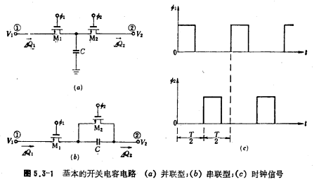
The switched capacitor circuit is a simple and basic circuit. It is composed of analog switches and capacitors. We can simulate it with an equivalent resistance. The basic parallel and series switched capacitor circuits are shown in Figure 5.3-1a, b As shown, they each contain a capacitor and two switches. Figure 5.3-1c shows the clock signal that controls the MOS switch.

(1) Working principle of switching filter circuit
(1) Working principle of switching filter circuit
Consider first the working condition of the circuit in Figure 5.3-1a. When the clock signal Ф1 is at high level and Ф2 is at low level, the M1 tube is turned on and the M2 tube is turned off, the input terminal voltage V1 charges the capacitor C, and the voltage across its two ends is V1. In the first half cycle, the voltage on capacitor C is V2, so the amount of charge charged to capacitor C at the input is ΔQ1=C (V1-V2); when Ф2 is high and Ф1 is low, M2 is turned on and M1 When the tube is cut off, the capacitor C is discharged, and the voltage across it is V2. Obviously, the discharge charge ΔQ2=C(V1-V2)=ΔQ1. The working principle of switched capacitor filter. Between each clock cycle T interval, the charge C (V1-V2) enters from node ① and flows out from node ②. We can define the average current  from node ① to node ② as

From this, the equivalent resistance  between node ① and node ② can be obtained as

Therefore, the function of the circuit in Figure 5.3-1a is equivalent to a resistance with a value of T/C.
The same analysis for the circuit in Figure 5.3-1b shows that this circuit can also be regarded as an equivalent resistance, and its value is also equal to T/C.
It must be pointed out that the circuit in Figure 5.3-1a and b should be equivalent to an analog resistor , Clock signal frequency
 Should be much larger than the working rate of the signal source V1 and V2.
(2) Switch circuit filter
If the resistance in the active RC filter is replaced by a switched capacitor circuit, a switched capacitor filter is formed. Obviously, the switched capacitor filter only contains op amps, switches, and capacitors. Assuming that the op amp and switch are ideal components, its frequency response characteristics only depend on the capacitance value. Formally, the time constant of R1C2 will be replaced by (T/C1)C2=(C2/C1)/fck, where C1 is used to replace the switch capacitor value of resistor R1, and fck is the clock frequency. As mentioned earlier, in the MOS process, the error of the capacitance ratio can be less than 1%. Therefore, the time constant of the integrated switched capacitor filter can reach an accuracy of 1% or better. In addition, when switching capacitors are used to implement large-value resistors, usually only a small silicon chip area is required. For example, when the capacitance is 1 picofarad and the clock signal frequency fck is 100 kilohertz, the equivalent resistance is 10 megohms. If a 10 megohm resistor is made directly on a silicon chip, the silicon chip area is 400 times the silicon chip area required to make a picofarad capacitor.
In addition to the basic switched capacitor circuit shown in Figure 5.3-1a and b, there is also a switched capacitor circuit as shown in Figure 5.3-2. For simplicity, the switches in the figure represent MOS transistor switches. Ф1 and Ф2 are shown in Figure 5.3-1 The clock signal shown must be high when Ф1 or Ф2, the switch is turned on, otherwise it is turned off. It can be proved that their equivalent analog resistance. The resistance values of are all equal to T/C, and the circuits in Figure 5.1-2a and c are equivalent to a negative resistance, that is 

2. Switched capacitor integrator
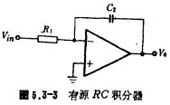
The active RC integrator shown in Figure 5.3-3 is the basic unit of an active RC filter. If the operational amplifier in the figure is ideal, the relationship between its input and output is
Using the Laplace transform and assuming that the initial state is zero, the above formula can be written as

Write the above equation in the form of a transfer function, and its expression is

In the formula, S is the Laplace transform variable, and R1C2 is the integration time constant of the integrator.
Under steady-state conditions, S=jω is substituted into (5.3-4), the transfer function can be expressed as

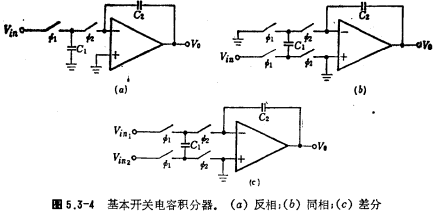
If the switch capacitor circuit shown in Figure 5.3-1 and Figure 5.3-2 is used to replace the integrating resistor 1 in the circuit of Figure 5.3-3, a switched capacitor integrator can be obtained. The basic circuit form is shown in Figure 5.3-4.

The equivalent resistance  of the switched capacitor in Figure 5.3-4a, replace this value with R1 in the equation (5.3-5), and get the transfer function of Figure (a) as


Where fck (1/T) is the frequency of the clock signal. From the formula (5.3-6), the input signal It has an inverted relationship with the output signal Vo, so the circuit in Figure (a) is an inverting switched capacitor integrator. The equivalent resistance
 of the switched capacitor in Figure (b), its transfer function is

It can be seen from the above formula that the circuit in Figure (b) is a non-inverting switched capacitor integrator. Now let's calculate the transfer function of the circuit in Figure 5.3-4c. The circuit has two input signals When it is zero (grounded), it is an inverting switched capacitor integrator, so its output voltage Vo and input voltage
 The relational formula is (5.3-6) formula;
 when it is zero (grounded), it is the same-phase switched capacitor integrator, the output voltage Vo and the input voltage
 The relational formula is (5.3-7) formula. According to the superposition theorem, the output voltage Vo of the circuit in Figure (c) and the input signal
 the relationship is

-fcx V.=-a (Vai-Va.), (5.3-8) Because the output voltage V is proportional to the difference between the input signal Vx and V2a, the circuit in Figure 5.3-4 (c) is a differential switch Capacitance integrator.

3. An integrator that does not count the parasitic capacitance
(1) The influence of parasitic capacitance on switched capacitor integrator
In the second section of Chapter 4, we discussed the structure of MOS capacitors. MOS capacitors have upper plate parasitic capacitance and lower plate parasitic capacitance. Because the capacitor in the switched capacitor integrator is a MOS capacitor made of MOS technology, it is necessary to discuss what effect the parasitic capacitance will have on the performance of the switched capacitor integrator, and how to reduce or eliminate the influence of the parasitic capacitance on the switched capacitor integrator. For MOS capacitors, the parasitic capacitance of the bottom plate is much greater than the capacitance of the top plate. In a switched capacitor integrator, in order to eliminate the influence of the parasitic capacitance of the bottom plate on the performance of the integrator, the bottom plate of the switched capacitor should be grounded or connected to a low-impedance power supply. For the integrating capacitor of the op amp, its bottom plate should be connected to the virtual ground of the output or input of the op amp. The influence of parasitic capacitance on the switched capacitor integrator is discussed below.
The circuit in Figure 5.3-5 is a commonly used differential switched capacitor integrator, which is the actual form of the circuit in Figure 5.3-4c. The MOS tubes M1, M2, M3 and M4 in the figure are switching tubes, and their gates are respectively connected with bi-phase clock signals ф1 and ф2. When ф1 is high, M1 and M2 are turned on, M3 and M4 are turned off, and the capacitor C1 And input signal source Turn on; when ф2 is high, M3 and M4 are turned on, M1 and M2 are turned off, and the capacitor C1 is connected to the input terminal of the operational amplifier. In the picture
 ,
, and
and they are the upper plate parasitic capacitance and the lower plate parasitic capacitance of the switched capacitor C1 and the integrating capacitor C2 respectively, and the influence of these parasitic capacitances will now be explained separately.
 the parasitic capacitance is connected to the output terminal of the op amp. Generally, the output impedance of the op amp is low, so this capacitance has little effect on the operation of the integrator.
 The parasitic capacitance is connected to the negative terminal of the input terminal of the op amp. If the gain of the op amp is high, the impact of this capacitor on the circuit can be ignored, because the inverting input terminal of the op amp is a virtual place, and its voltage is approximately zero.
 The parasitic capacitance is the capacitance from the bottom plate of the capacitor C1 to the ground, and it has no effect on the operation of the integrator, because it is either connected to the image.png signal source or connected to the ground.
 The parasitic capacitance is the capacitance from the upper plate of the C1 capacitor to the ground. This capacitance is connected to the switch
 when, it needs to store charge on it
 , When the switch is connected to the input terminal of the op amp, this part of the charge will also be transferred to the integrating capacitor C2, so this capacitor has an impact.

In summary, of the four parasitic capacitances, only the parasitic capacitance of Cp1 affects the integrator. Consider the influence of parasitic capacitance. Then the transfer function of Figure 5.3-5 is

Compared with the formula (5.3-8), the above formula adds the error term introduced by Cp1. If C2 is much larger than Cp1, then the influence of Cp2 will be smaller. Obviously, it can be seen from (5.3-9) that when at this time, it belongs to the case of the in-phase integrator, and the integrator is not affected by the parasitic capacitance. If working in the differential state or phase inversion state, the parasitic capacitance Cp1 has an impact on the output of the integrator. In order to reduce this impact, C2 should be much larger than Cp1. In actual circuits, this condition is usually met.
(2) Parasitic capacitance insensitive switched capacitance integrator
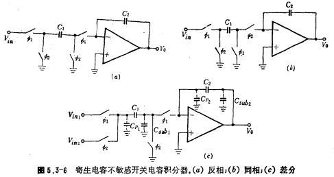
In order to completely eliminate the influence of parasitic capacitance on the integrator, the switched capacitor circuit can adopt the circuit form shown in Figure 5.3-2b and c. The switched capacitor integrator composed of the circuits in Figure 5.3-2b and c is shown in Figure 5.3-6a and c. Figure (a) is an inverting integrator; Figure (b) is an in-phase integrator; (c) is a differential integrator . Their transfer functions correspond to (5.3-6~8) respectively. It is easy to prove that the parasitic capacitances of capacitors C1 and C2 have no effect on the transfer function of the circuit in Figure 5.3-6. Now take the circuit in Figure 5.3-6(c) as an example. When ф1 is high, one end of the capacitor C1 is connected to the input signal source ,The other end is connected to the negative end of the op amp (ie virtual ground); when ф2 is high, one end of the capacitor C1 is connected to the input signal source
 ,The other end is grounded. Since the parasitic capacitance Cp1 is connected to a low impedance source, the parasitic capacitance
 , Ground or virtual ground, so Cp1,
 The parasitic capacitance has no effect on the working state of the integrator. Parasitic capacitance of capacitor C2
 ,They are also connected to the virtual place and the low output impedance source respectively, and they do not affect the output of the integrator. Therefore, the circuit in Figure 5.3-6c is a parasitic capacitance insensitive integrator. The same analysis shows that the circuits in Figure 5.3-6a and b are also parasitic capacitance insensitive integrators.

4. Design method of switched capacitor filter
At present, the more commonly used design methods of switched capacitor filters are mainly as follows:
(1) List the voltage and current equations of the passive RLC ladder filter nodes and branches. According to this equation, the signal flow diagram is given. The circuit structure of the switched capacitor filter is obtained from the signal flow diagram. The component values are directly determined by the RLC The inductance L, the capacitance C and the clock signal frequency fck in the ladder filter are determined. Switched capacitor filter design method. This design method has the advantages of simple circuit structure and low sensitivity, and it is easy to design high-order filters.
(2) The biquad RC active filter (the filter with the multi-op amplifier structure in the second section of this chapter) is directly derived from the biquad switched capacitor filter, and this circuit is cascaded to achieve high-order switched capacitor filtering Device. The advantage of using this design method is that a double second-order standard module can be used to design various filters such as low pass, high pass, band pass and band stop, which greatly simplifies the design.
Contact: Mr. Zou
Contact number: 0755-83888366-8022
Mobile phone: 18123972950
QQ: 2880195519
Contact Address: 5C1, Block CD, Tianji Building, Tianan Digital City, Chegongmiao, Futian District, Shenzhen
Please search WeChat official account: "KIA Semiconductor" or scan the following picture to "Follow" official WeChat official account
Please "follow" the official WeChat account: provide MOS tube technical assistance


