Electronic Technology Forum
Analysis of the Transformation Properties of Band Rejection Filter from Low Pass to Band Rejection
1. Conversion from low-pass to band-stop
Designing a band-pass filter also utilizes the geometric transformation from low-pass to band-stop. The transformation method is to replace the variable S in the low-pass transfer function with SB/(S2+ω2). After changing the prognosis in this way, the band-stop center angular frequency is ωo, the 3dB bandwidth is B, and the band-stop  is obtained. The value is the band-stop transfer function of fo/B. After the conversion from low pass to band stop, the amplitude-frequency characteristics of low-pass and band stop are shown in Figure 5.2-16.
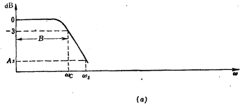
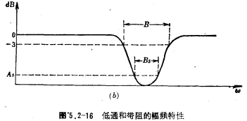
The attenuation characteristic of the band stop can be represented by the attenuation characteristic of the low pass. The normalized low-pass cut-off angular frequency Ωs is

After changing from low-pass to band-stop, its order doubles.
The second-order band-stop transfer function is expressed as

In the formula,  is the zero-point angular frequency.
(1) Conversion from second-order low-pass to band-stop
If the coefficient of the second-order low-pass transfer function is (See the equations (5.1-9), (5.1-12), (5.1-23) and (5.1-24) in the first section), and use S in the second-order low-pass transfer function with SB/(S2+ After ω2o) is replaced, the transfer function of the band-stop is obtained, which is expressed as

In the formula is the zero angular frequency. That
 And Q calculation steps:
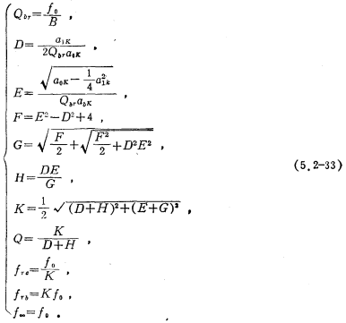
(2) First-order low-pass to stop-band conversion
If the real pole of the first-order low-pass is , Replace S in the first-order low-pass transfer function with SB/(S2+ω2o) to obtain the band-stop transfer function, the expression is (5.2-31), where:

[Example 8] Design a band stop filter, the main indicators are: (1) band stop center frequency fo=3600 Hz, (2) band stop filter 3 dB bandwidth B=300 Hz, (3) attenuation As is 40 dB When the stop band width Bs=60 Hz.
Solution i. Calculate the normalized low-pass stopband angular frequency Ωs:

ii. Calculate the order n according to the value of Ωs and As:
Choose the Chebylev approximation with RP=0.1dB. From the first section (5.1-19), the low-pass order n=3. Chebyshev coefficient the value is obtained after conversion from the value provided in Table 5.1-3

iii. According to ,Calculate Q,
 and
and :
:
Using the formula (5.2-33), we have
Q=30.15, =3455 Hz;
 =3752 Hz;
 Hz;
Hz;
iv. Calculate Q according to σo, andfr:

Ⅴ. The block diagram of the three-stage band rejection filter and its parameters are shown in Figure 5.2-17.

2. Multi-op amp band stop filter
The circuit form of the multi-op-amp band-stop filter is shown in Figure 5.2-18.
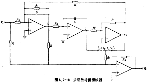
like 、Qand
、Qand It has been found that C, R and R′ in the figure can be selected arbitrarily, and the design formula of the circuit is

for

for

in The value is given when the DC gain is equal to 1. To increase or decrease the DC gain, you can change
 the resistance value to achieve.
The main advantage of the circuit in Figure 5.2-18 is that the Q value can be as high as 200, and the Q value and fr can be adjusted independently. It applies to the band rejection filter, such as the first and second stage band rejection filters of [Example 8], can use the circuit shown in Figure 5.2-18.
3. Band stop filter composed of band pass filter
for the band rejection filter (produced by the real pole) can be realized by the circuit structure of Fig. 5.2-19, where H(S) is the transfer function of the band pass. The input signal is divided into two channels, one of which is added to the inverting input end of the op amp after passing through the band-pass amplifier, and the gain is 1; the other is directly added to the non-inverting input end of the op amp, and the gain is also 1. These two signals are output after being added by the operational amplifier. The output characteristic is band-resistance, and the transfer function of band-pass is

So the transfer function of the circuit in Figure 5.2-19 is
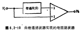
It means the transfer function of the time band stop wave device.
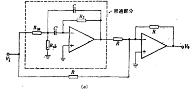
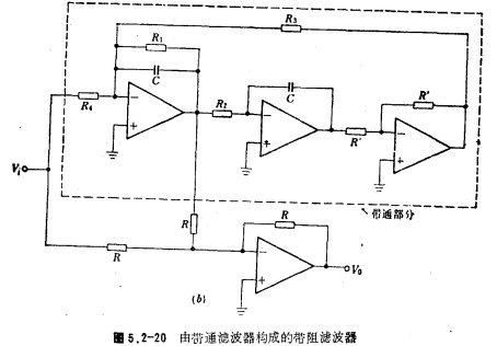
According to the circuit structure of Figure 5.2-19, a band-stop filter composed of a band-pass filter can be obtained. The circuit form is shown in Figure 5.2-20. Figure (a) is a multi-channel feedback band-pass filter; Figure (b) It is a multi-op-amp band-pass filter. The center frequency of these band-stop filters is the same as the center frequency of the band-pass filter. With bandpass
 same. The design formula of its component value has been discussed in the band pass filter, and will not be repeated here (the design formula can be viewed by clicking here). The circuit in Figure 5.2-20 can be used as the third-stage band-stop filter in [Example 8].
4. Double T band stop filter
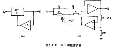
The double T network is often used in the band rejection filter. The Q value of the passive double T network is only 1/4. In order to improve the Q value of the double-T band rejection filter, positive feedback can be used. The circuit form is shown in Figure 5.2-21a. The β in the figure is a double-T network and K is an amplifier. After calculation, its Q value

In the formula, K is less than 1 and close to 1, the larger the K, the larger the Q value. Figure 5.2-21b shows the actual circuit with a positive feedback double T band stop filter. The design formula of this circuit is

Where fo is the center frequency of the band stop, and the corresponding attenuation value As of the stop band width Bs is

It can be seen from the above formula that the larger the Q, the smaller the attenuation value As under the same Bs condition,
[Example 11] Design a double T band stop filter, the main parameters: (1) band stop center frequency fo=50 Hz; (2) Q=5.
Solution Choose capacitance C=0.01 microfarads. By (5.2-40) formula

By (5.2-41) formula

In the figure, R is 100 kiloohms, then (1-K) R=5 kilograms, and K R=95 kiloohms. If Bs=1 Hz, then As=20 decibels.
Contact: Mr. Zou
Contact number: 0755-83888366-8022
Mobile phone: 18123972950
QQ: 2880195519
Contact Address: 5C1, Block CD, Tianji Building, Tianan Digital City, Chegongmiao, Futian District, Shenzhen
Please search WeChat official account: "KIA Semiconductor" or scan the following picture to "Follow" official WeChat official account
Please "follow" the official WeChat account: provide MOS tube technical assistance


