Electronic Technology Forum
Detailed analysis of band-pass filter circuit and conversion formula multi-channel feedback
1. Conversion from low pass to band pass
The most common way to design a band-pass filter is to use the geometric transformation from low-pass to band-pass. The method is to use the variable S in the low-pass transfer function with Instead, after this transformation, the bandpass transfer function with the center angular frequency of ωo and the 3dB bandwidth of B is obtained. After changing from low-pass to band-pass, the relationship between the low-pass amplitude-frequency characteristics and the band-pass amplitude-frequency characteristics is shown in Figure 5.2-11.
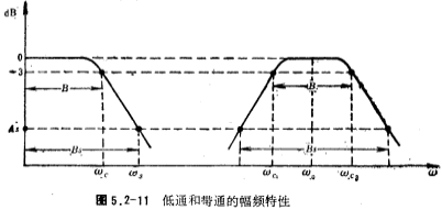
In the figure, ωo, ωc1, and ωc2 are the center angular frequency of the band-pass filter and the angular frequency when it drops by 3 decibels. The band-pass coal degree B=ωc2-ωc1, the center angular frequency .Bs is the stop width of the band pass. Band pass filter circuit. It can be seen from the figure that the band-pass width B is the same as the low-pass bandwidth, so the attenuation characteristic of the band-pass can be represented by the attenuation characteristic of the low-pass, that is, the normalized low-pass cutoff angular frequency Ωs is

Generally speaking, the low-pass transfer function is K-order, and the transformed band-pass transfer function is 2K-order. Therefore, the order of the band-pass filter is only even-order, no odd-order, and the lowest order is second-order.
2. Conversion formula from low-pass to constant-pass
The second-order bandpass transfer function can be written as

In the formula, Ar, ωr, Q are the gain, center angle frequency and Q value of the second-order bandpass respectively.
(1) First-order low-pass to band-pass conversion
If the real pole of the first-order low-pass is image.png, use S in the first-order low-pass transfer function Instead, the second-order band-pass transfer function is obtained, namely (5.2-14), where ωr=ωo,

and

(2) Second-order low-pass to band-pass conversion
If the second-order low-pass transfer function has coefficients (See the equations (5.1-9), (5.1-12), (5.1-23) and (5.1-24) in the first section), and use S in the second-order low-pass transfer function
 Instead, the transfer function of the second-order band-pass filter is obtained

Where So and Q are the gain, resonant frequency and Q value of the second-order bandpass filter, respectively. The calculation steps of
  and Q are as follows:
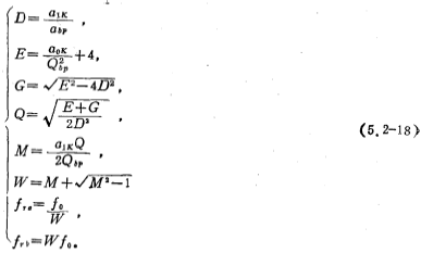
(3) The relationship between single-stage band-pass filter gain Ar and Ao
When the single-stage band-pass filter is at the center frequency fo, its gain is Ao, and when the single-stage band-pass filter is at the resonance frequency fr, its gain is Ao.
Gain is the relationship is

[Example 5] Design a sixth-order Butterworth band-pass filter, the main indicators: (1) center frequency fo=1000 Hz, (2) 3 dB bandwidth B=100 Hz, (3) intermediate frequency gain Ao=30 dB.
Solution i. Calculation

ii. Calculation :
:
From the formula (5.1-12) and Table 5.1-1, when n=3, for
for

iii. by
From (5.2-18) formula
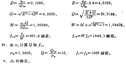
This band-pass filter is composed of three second-order band-pass filters, the mid-frequency gain (when fo) is 30 decibels, and the gain of each stage is set to 10 decibels, that is, Ao=3.162. By (5.2-19), the gain Ar of each stage is obtained.
vi. The parameters of the second-order band pass filter at all levels:
The first level: fr=957.6 Hz, Q=20.02, Ar=6.333.
The second level: fr=1044.3 Hz, Q=20.02, Ar=6.335.
The third level: fr=1000, 0 Hz, Q=10.00, Ar=3.162.
3. Filter sensitivity
RC active filter changes due to changes in the resistance, capacitance value or the gain of the op amp, so that the filter parameter Q value, the center frequency fo of the band pass, etc. change. The sensitivity is usually used to measure the effect of the change of the component parameters on the filter parameters. Influence. Band pass filter circuit. If x is used to represent a certain element (resistance, capacitance, and operational amplifier gain), and y represents a certain filter parameter, the sensitivity of y to changes in x is defined as

In the band-pass filter, the sensitivity index directly reflects the stability of the band-pass center frequency fo and bandwidth B. The lower the sensitivity, the better the stability of the filter parameters, so it is a more important parameter.
4. Multi-channel feedback band pass filter
The multi-channel feedback bandpass filter is shown in Figure 5.2-12. It has the characteristics of simple circuit structure and low sensitivity. The transfer function of the circuit in Figure 5.2-12 (a) is (see Reference (31))

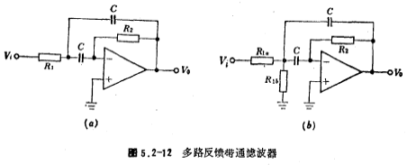
If the coefficients of (5.2-21) are equal to those of the general bandpass transfer function (5.2-14), the relationship between the component values of the circuit in Figure 5.2-12a and the bandpass parameters can be obtained:

The value of capacitance C is arbitrary in the formula.
The disadvantage of this circuit is that Ar is proportional to the square of Q, so the value of Q cannot be too large, usually Q should be below 20. picture
5.2-12b is its improved form, and the corresponding transfer function is (see Reference (31))

where the relationship with Ar and Q is

In the formula, Ar is the required gain at the resonant frequency fr, but it cannot be greater than 2Q2. Band pass filter circuit. The relational expression of R2 in the figure is still expressed by (5.2-22). The sensitivity of the circuit is expressed by the following equations
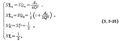
Under the condition of Q2/Ar》1, the Q value of the resonant frequency fr circuit can be directly controlled by R10, which means changing the resonant frequency fr. The Q value of the circuit can be adjusted by R2.
[Example 6] Use the circuit of Figure 5.2-12b with multiple feedback band-pass filters to realize the sixth-order Butterworth band-pass filter designed in [Example 5].
Solution i. According to the calculation in [Example 5], the structure and parameters of the sixth-order Butterworth bandpass filter are shown in Figure 5.2-13.

ii. Calculate the component values in the circuit of Figure 5.2-12b:
Choose capacitance C=0.01 microfarads.
Component value of the first stage resistor
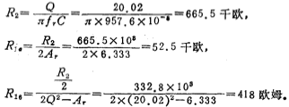
Component value of second-level resistor

Component value of the tertiary resistor

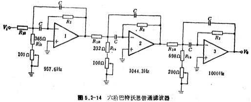
iii. Sixth-order Butterworth bandpass filter circuit: The actual circuit of the sixth-order Butterworth bandpass filter is shown in Figure 5.2-14.
The in the picture is a series of trimming resistors to adjust the resonant frequency fr of each band-pass filter so that the center frequency fo of the band-pass filter is 1000 Hz. Band pass filter circuit. The other resistance values of each level are as calculated above. The capacitance C is 0.01 microfarads.
5. Multi-op amp bandpass filter
The multi-op amp bandpass filter is shown in Figure 5.2-15. The circuit has very low sensitivity, and the Q value of the circuit and the resonant frequency fr can be adjusted independently without affecting each other. It is particularly suitable for making a standard form of high-precision active filter. If the integrated four-op-amp circuit is used, the volume can be made small. The transfer function of the circuit in Figure 5.2-15 is

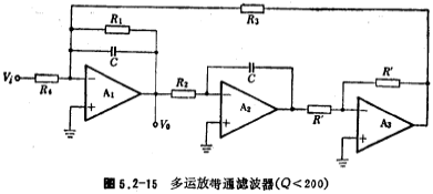
Let the above formula and the second-order bandpass transfer function (5.2-14) be equal, then the resonant frequency fr and bandwidth B of the circuit are

From the equation (5.2-27), we can see that the resonance frequency fr and the 3dB bandwidth B can be adjusted independently.
Assume ,then from (5.2-26) formula and (5.2-27) formula, the circuit design formula can be obtained

In the formula, Ar is the required gain at the resonant frequency fr. Band pass filter circuit. The capacitance C value and the resistance R'value in the circuit in Figure 5.2-15 can be selected arbitrarily. From the equation (5.2-28), it can be seen that the function of R2 is to adjust the resonant frequency fr of the circuit, the function of R1 is to adjust the Q value of the circuit, and the function of is to adjust the gain Ar. The circuit sensitivity is

where is the open loop gain of amplifiers A1 and A2. The Q value is limited by the open loop gain of the op amp. Rock chooses a high gain op amp, and the Q value can reach 200.
[Example 7] Design an active bandpass filter, the main parameters are: (l) center frequency fo=2500 Hz, (2) 3dB bandwidth B=30 Hz, (3) when attenuation A≥15dB, stop band Bandwidth Bs=90 Hz, (4) At 2500 Hz, the gain is 12 decibels.
Solution i. Calculate the normalized low-pass stopband angular frequency Ωs:

ii. Determine the low-pass order:
Choose n=2 =0.1dB Chebyshev low-pass filter meets its stop-band attenuation requirements.
iii. Calculation :
:
From Table 5.1-3, we have

iv. Calculation
From the formula (5.2-18)

v. Optional circuit:
This circuit has a very high Q value. The circuit structure shown in Figure 5.2-15 is used. Because the band-pass order n is equal to the fourth-order, a two-stage multi-op-amp band-pass filter is required.
vi. Gain distribution:
The total gain is 12 decibels, and the gain of each stage is 6 decibels, that is, Ao=2. Using the formula (5.2-19), the gains of the first and second stages Ar=3.069.
vii. The parameters of the first and second stages of the band pass filter:
The first level: fr=2489.3 Hz, Q=136, Ar=3.069.
The second level: fr=2510.7 impressively, Q=136, Ar=3.069.
viii. Calculate the component values of the first and second stages of the bandpass filter:
Choose C=0.1 microfarad; R'=10 kiloohms.
First level:
The second level: R1=86.2 kiloohms, R2=R2=64 kiloohms, R4=28.1 kiloohms.
Contact: Mr. Zou
Contact number: 0755-83888366-8022
Mobile phone: 18123972950
QQ: 2880195519
Contact Address: 5C1, Block CD, Tianji Building, Tianan Digital City, Chegongmiao, Futian District, Shenzhen
Please search WeChat official account: "KIA Semiconductor" or scan the following picture to "Follow" official WeChat official account
Please "follow" the official WeChat account: provide MOS tube technical assistance


