Electronic Technology Forum
MOS operational amplifier active low-pass filter design and size principle circuit detailed explanation
1. Second-order and third-order low-pass active filters
Figure 5.2-1a and b are the second-order and third-order low-pass active filters respectively. They form a full feedback form, so they have low output impedance and high input impedance. Therefore, when this circuit is used in cascade, the level There is no impact between the and stages, that is to say, using the circuit in Figure 5.2-1a and b as the basic unit, the cascade connection can easily realize the high-order low-pass active filter.

For convenience, the resistance values in the figure are assumed to be 1 ohm.
Figure 5.2-1a The transfer function H(S) of the second-order low-pass active filter is

If you choose a normalized Butterworth low-pass filter, compare (5.2-1) with the Butterworth network function (5.1-9), and make the coefficients of the two equations equal, so you can get

From Table 5.1-1,  .414, substituting into the above formula, we get

Here, the units of C1 and C2 are farads.
If normalized with a Chebyshev low-pass filter of 0.5 decibels, compare the formula (5.2-1) with the Chebyshev network function (5.1-23), make the coefficients of the two formulas equal, and use the values in Table 5.1-5. After conversion, the capacitance values of C1 and C2 are: C1=1.403, C2=0.470.
For the capacitors C1, C2, and C3 in the third-order low-pass active filter in Figure 5.2-1b, the same method can be used to obtain the values.
Tables 5.2-1~4 list the capacitor values in the low-pass filter in Figure 5.2-1 according to Butterworth and Chebyshev network functions.


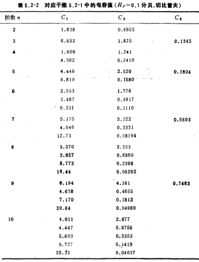
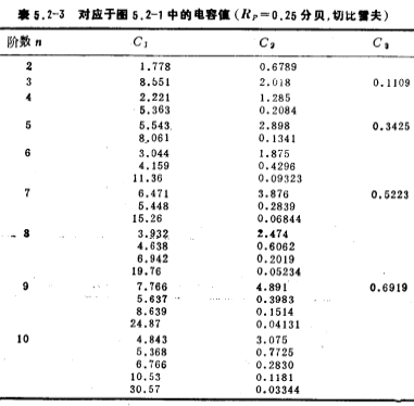
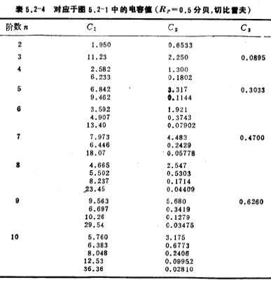
We use the circuit in Figure 5.2-1 and the capacitance values in Tables 5.2-1~4 to easily design a Butterworth or Chebyshev low-pass filter.
[Example 1] Design a normalized pentavalent Butterworth low-pass filter.
Using the circuit structure shown in Figure 5.2-1a, b, the third-order low-pass filter and the second-order low-pass filter are connected in series to form a fifth-order low-pass filter. The connection method is shown in Figure 5.2-2.

From Table 5.2-1, the values of capacitors C1, C2, and C3 of the first stage (third-order low-pass filter) in the circuit of Figure 5.2-2 are: C1=1.753 Farads, C2=1.354 Farads, C3=0.4214 Farah. Similarly, from Table 5.2-1, the values of the capacitors C1 and C2 of the second stage (second-order low-pass filter) of the circuit are: C1=3.235 Farads, C2=0.3090 Farads.
The low-pass filter designed above is obtained under the condition of normalized frequency, and the selected resistance value is very small, and the capacitance value is very large, which is not suitable for the actual situation. Therefore, it is necessary to perform frequency conversion according to the actual operating frequency, and the resistance and capacitance in the circuit must also be scaled.
2. Scale transformation
Suppose the frequency conversion factor is FSF, which is defined as

If the cut-off frequency of the low-pass filter fc=100 Hz and the normalized cut-off angle frequency Ω=1 radian/sec, the frequency conversion factor FSF is

For a normalized low-pass filter, the cut-off angle whisker rate Ω=1 radian/s, if you want to convert to a certain cut-off whisker rate fc, then the capacitor value in the normalized low-pass filter should be divided by The factor value FSF is transformed by frequency.
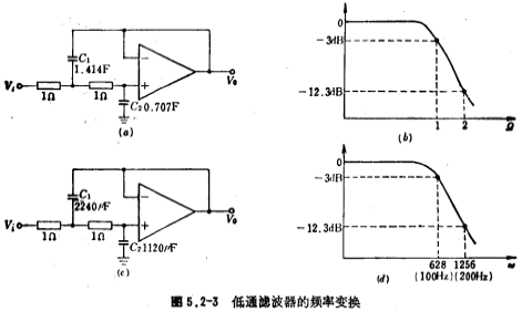
Figure 5.2-3 shows an example of frequency conversion, Figure 5.2-3a is a second-order normalized Butterworth low-pass filter, and Figure 5.2-3b is its amplitude-frequency characteristics. Figure 5.2-3(c) is a second-order Butterworth low-pass filter with a cutoff frequency fc of 100 Hz. Its capacitance value is 1/628 of the capacitance value in the circuit of Figure 5.2-3a, and Figure 5.2-3d is its Amplitude frequency characteristics.
In addition to frequency conversion, the resistance value and capacitance value also need to be scaled. Suppose the scale conversion factor of impedance is Z. If we increase the resistance in the filter by a factor of Z, then all the impedances in the entire network should be increased by a factor of Z. To increase the capacitive reactance of the capacitor by a factor of Z, the value of the capacitor should be reduced by a factor of Z. Therefore, the scale transformation relationship between the resistance and the capacitance in the filter is

Now, the resistance and capacitance in the second-order Butterworth low-pass filter in Figure 5.2-3c are transformed into impedance scale. If Z=10000, the resistance value in the figure is R'=ZR=10 kiloohms, and the capacitance value is C1' =C1/Z=0.224 microfarads, C2'=C2/Z=0.112 microfarads. After impedance scale transformation, its amplitude-frequency characteristics remain unchanged.
After comprehensive consideration of frequency transformation and impedance scale transformation, the relationship between resistance and capacitance transformation is
[Example 2] Design a low-pass filter with a gain of 1, the main indicators are: (1) Cut-off frequency fc=100 Hz; (2) When the stop band frequency fc=350 Hz, the attenuatio decibels; (3) the passband fluctuation is not more than 0.5 decibels.
Solution i. Calculate the stop band normalized angular frequency Ωs:

ii. Optional Decibel Chebyshev low-pass filter;
iii. Find the order n from the formula (5.1-19);
will the value is substituted into the formula (5.1-19), and the order n=5;
iv. Choose the circuit structure shown in Figure 5.2-2;
v. Use Table 5.2-4 to get the normalization decibel Chebyshev low-pass filter. The capacitance value of the first stage filter is
C1=6.842 farads, C2=3.317 farads, C3=0.303 farads.
The capacitance value of the second stage filter is
C1=9.462 Farads, C2=0.114 Farads.
vi. Perform color rate conversion and impedance scale conversion;
FSF=628, take Z=5×10⁴.
The capacitance and resistance of the first-stage filter;


Capacitance value and resistance value of the second stage filter:
C1'=0.301 microfarads, C2'=0.00363 microfarads, R'=50 kiloohms
The low-pass filter that meets the design specifications and its amplitude and whisker characteristics are shown in Figure 5.2-4a and b.

3. Design of low-pass filter
From the above discussion, it is easy to design low-pass filters of different orders by using the circuit shown in Figure 5.2-1. However, the capacitance value designed by this circuit structure often deviates from the standard value, and the capacitance value is different. It often brings difficulties to design and production personnel. For this, you can choose the second-order low-pass filter circuit shown in Figure 5.2-5, with a gain of 2. The capacitance value in the figure can be selected by the designer. To achieve a high-order (n is an even number) low-pass filter, the circuit of Figure 5.2-5 can be connected in series.
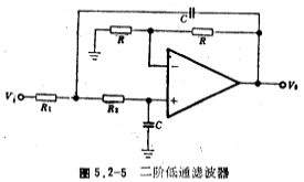
The design formula of the second-order low-pass filter shown in Figure 5.2-5 is:
(1) Determine the capacitance value (selected by the designer)

where Are the coefficients of Butterworth and Chebyshev network functions (see equations (5.1-9), (5.1-12), (5.1-23) and (5.1-24)), and their values are shown in Tables 5.1-1~5, respectively Figure 5.2-5 shows the second-order low-pass filter. For Butterworth low-pass filter, its
 ; Ωc is the cut-off corner frequency of the low-pass filter.
The resistance value obtained from equations (5.2-7) and (5.2-8) is not a normalized value, but a value after frequency transformation and impedance scale transformation.
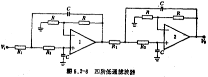
[Example 3] Design a passband fluctuation it is a fourth-order Chebyshev low-pass filter with a cut-off frequency of fc of 100 Hz and 0.1 decibel.
Solution i. Use the circuit structure shown in Figure 5.2-5. The circuit form of the fourth-order Chebyshev low-pass filter is shown in Figure 5.2-6.
ii. Choose capacitance C=0.01 microfarad.
iii. Obtained from Table 5.1-3

iv. Calculate R1 and R2;
First level ;
;

second level

v. The resistance R in the figure can be selected as 100 kiloohms.
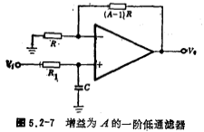
For a low-pass filter with an odd order, there must be a real pole , It can be realized by a first-order low-pass filter with a gain of A, and its circuit form is shown in Figure 5.2-7. The resistance value R1 in the figure can be obtained by the following formula;

Where fc is the cut-off rate of the low-pass filter, It is the real pole. The resistance R1 value obtained by the above formula is not a normalized resistance value, but a resistance value after frequency transformation and impedance scale transformation.
For Butterworth low-pass filters, the poles are actually =1, And the poles of the Chebyshev low-pass filter can be found in Tables 5.1-3~5.
The odd-order low-pass filter can be realized by connecting the circuit of Figure 5.2-7 and Figure 5.2-5, or in series with the circuit of Figure 5.2-1a, that is, the first stage of the odd-order low-pass filter is a first-order low-pass filter. The following stages are second-order low-pass filters.
Contact: Mr. Zou
Contact number: 0755-83888366-8022
Mobile phone: 18123972950
QQ: 2880195519
Contact Address: 5C1, Block CD, Tianji Building, Tianan Digital City, Chegongmiao, Futian District, Shenzhen
Please search WeChat official account: "KIA Semiconductor" or scan the following picture to "Follow" official WeChat official account
Please "follow" the official WeChat account: provide MOS tube technical assistance


