Electronic Technology Forum
Typical example of silicon gate CMOS operational amplifier layout design
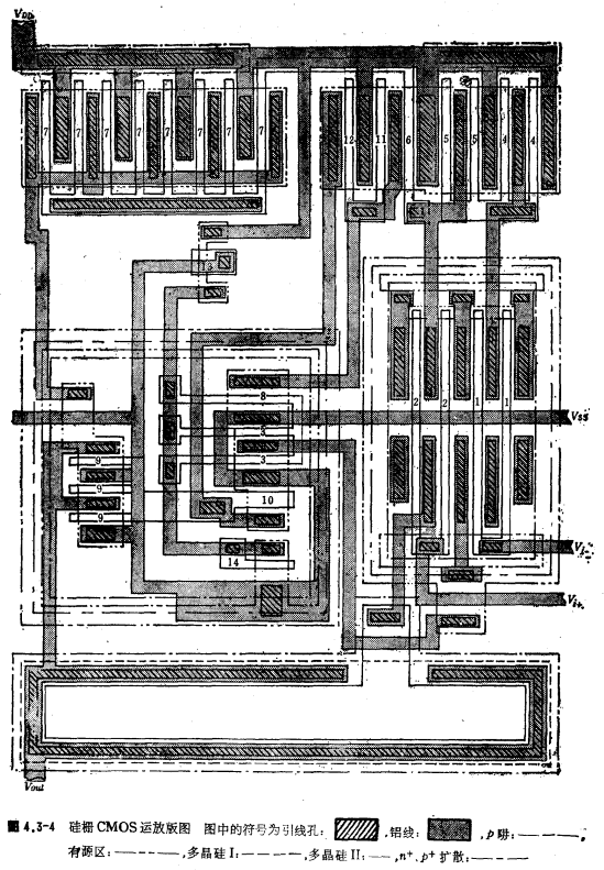
An example of the layout of a silicon gate CMOS op amp is shown in Figure 4.3-4. The circuit diagram shown in this layout is the CMOS op amp shown in Figure 3.11-7 in Chapter 3. The serial number in the layout corresponds to the serial number of the tube in the circuit in Figure 3.11-7.
In the figure, the M1 and M2 input tubes are made in a P-well, and the P-well potential is connected to the sources of the two tubes from the P+ ring, that is, the M1 and M2 tubes pass through independent P-wells to short-circuit the substrate and the source to reduce Small substrate bias effect. Other n-channel MOS tubes are all made in another P well. The P-channel MOS tube is fabricated on the n-substrate outside the P well. The compensation capacitor Co in the figure is composed of double-layer polysilicon.

The layout shown in Figure 4.3-4 has eleven sets of photoengraved plates. They are:
(1) P-well lithography plate.
(2) Active area photolithography.
(3) Polysilicon I lithography plate. Polysilicon I serves as the bottom electrode of the MOS capacitor.
(4) N-channel field injection photolithography. In this process, boron is injected into the n-channel field area to increase the field turn-on voltage of the n-channel field area . Before the n-channel field implantation, the active area has been masked by Si3N4, and boron ions will not be injected into the active area. Therefore, the n-channel field implantation lithography can be used with the P-well lithography.
(5) Threshold voltage of P-channel MOS tube adjust the lithography plate, this lithography plate uses the reverse version of the P well.
(6) Multi-product silicon II photolithography plate. This process forms the gate of the MOS transistor and the upper electrode of the multi-layer polysilicon capacitor.
(7) P+ zone photolithography.
(8) n+ zone lithography plate, that is, the reverse version of p+ zone lithography plate.
(9) Lead hole photoengraved plate.
(10) Aluminium strip lithography.
(11) Passivation lithography.
The op amp layout shown in Figure 4.3-4 is 500 times the actual layout (chip size), and the minimum channel length of the MOS tube is micrometers.
Contact: Mr. Zou
Contact number: 0755-83888366-8022
Mobile phone: 18123972950
QQ: 2880195519
Contact Address: 5C1, Block CD, Tianji Building, Tianan Digital City, Chegongmiao, Futian District, Shenzhen
Please search WeChat official account: "KIA Semiconductor" or scan the following picture to "Follow" official WeChat official account
Please "follow" the official WeChat account: provide MOS tube technical assistance


