Electronic Technology Forum
6-micron design rule and layout analysis of silicon gate CMOS process
According to the first section (5), the nine lithography plates used in the planar isolation CMOS process steps such as silicon gates are formulated as follows (some rules considering the same starting point as aluminum gates will not be explained):
1. P-well version
The minimum distance between P well and P well is 26 microns.
2. Active area version
(1) The minimum width of the active area is 6 microns.
(2) The minimum interval between active areas is 8 microns.
(3) The minimum distance between the P+ active area outside the P well and the P well is 20 microns.
(4) The minimum distance between the n+ active region outside the P well and the P well is 10 microns.
(5) The n+ active region in the P-well is 10 microns away from the P-well.
(6) The inner side of the P+ ring active area around the P well, the distance from the P well is 2 microns, and the outer side of the P+ ring active area is 4 microns from the P well.
3. N-channel field injection version
The n-channel field implantation area is 4 microns larger than the p-well area to ensure that the surface of the p-well area will not be inverted.
4. Polysilicon version
(1) The minimum width of polysilicon is 6 microns.
(2) The minimum distance between polysilicon is 6 microns, because there is no need to consider lateral diffusion between polysilicon. Silicon gate CMOS process 6 micron design.
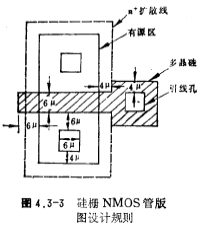
(3) When polysilicon overlaps with the diffusion area to form a MOS tube area, the polysilicon must extend 6 microns from the active area to ensure that there is indeed a gate electrode potential control on the channel area between the drain and the source to prevent the drain between the source and the source. Direct short circuit. As shown in Figure 4.3-3.

(4) In the non-MOS tube area, the distance between the polysilicon and the active area is 4 microns. Otherwise, when the photolithography is not registered, the overlap of the polysilicon and the diffusion area will form an unnecessary MOS capacitor. Silicon gate CMOS process 6 micron design.
5. Adjusted version of P groove threshold voltage VT
The P-channel VT adjustment version must be at least 4 microns larger than the P-channel MOS tube channel area, and it can be a reverse version of P-well or n-channel field implantation.
6, n+ diffusion layout design rules
The n+ diffused version is at least 4 microns larger than the n+ active area.
7, p+ diffusion version
The p+ diffused version is at least 4 microns larger than the p+ active area, and in fact the n+ reverse version can be used.
8. Lead hole plate
(1) The minimum distance between the lead hole on the active area and the boundary of the active area is 4 microns.
(2) The minimum distance between the lead hole on the active area and the polysilicon gate is 6 microns.
(3) The minimum distance between the lead hole on the polysilicon and the boundary of the polysilicon is 4 microns.
(4) The minimum size of the lead hole is 6 μm×6 μm or 4 μm×8 μm.
9. Aluminum strip lithography
(1) The minimum width of the aluminum bar is 6 microns.
(2) The minimum spacing between aluminum bars is 6 microns.
(3) The aluminum strip covers the lead hole by 2 microns.
Contact: Mr. Zou
Contact number: 0755-83888366-8022
Mobile phone: 18123972950
QQ: 2880195519
Contact Address: 5C1, Block CD, Tianji Building, Tianan Digital City, Chegongmiao, Futian District, Shenzhen
Please search WeChat official account: "KIA Semiconductor" or scan the following picture to "Follow" official WeChat official account
Please "follow" the official WeChat account: provide MOS tube technical assistance


