Electronic Technology Forum
Aluminum gate CMOS process design rules-(six lithography plates) detailed rules
Aluminum gate CMOS process design rules
The layout design rules of CMOS circuits are the same as those of other circuits. First, consider the minimum size and minimum spacing allowed by the photolithography process, such as the minimum size and spacing of the diffusion area, the minimum size and spacing of polysilicon, and the minimum size of aluminum bars. And intervals and so on. Secondly, we must consider the allowable registration accuracy between the lithography plates. In addition, from the perspective of device performance, it is necessary to formulate the minimum allowable dimensions of some devices, such as channel length, etc. In order to reduce some parasitic effects and leakage in CMOS circuits, it is necessary to formulate some rules for tube spacing when designing the layout.
Since design rules are closely related to process conditions and process levels, the design rules of each unit can be different. With the continuous improvement of process levels, the design rules will continue to improve, so the data in the design rules listed below is just an example. Mainly put forward the issues that should be considered in the design rules, as a reference for formulating design rules.
Referring to the first section of the aluminum shed CMOS process flow, we know that the aluminum gate CMOS process requires a total of six photolithography plates, and the design rules of each photolithography plate should be considered as follows:
1. P-trap lithography
(1) The minimum width of the P-well region is generally not specified, because an n-channel tube is to be made in the P-well region. In fact, the width of the p-well is always relatively large and will not be restricted by the photolithography process.
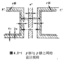
(2) The minimum distance between P well and P well is 40 microns
In the CMOS process, the substrate potentials of the NMOS field effect transistors are generally the same, and they can be made in a P well. when
When the substrate potential of the NMOS tube is not the same, the P well must be separated. Aluminum gate CMOS process design rules. Because the junction of the P-well is deeper , So its lateral diffusion is also larger (6~8 microns), and considering the expansion of the barrier when the p-n-junction is reverse-biased, the distance between the P-wells should be larger. In fact, in order to prevent the field opening leakage between the P well and the P well, an n+ isolation ring must be made on the n- substrate between the two P wells, and there is a P+ ring around the P well, so the distance between the P wells is 40 microns, as shown in Figure 4.3-1.


2. P+ zone lithography
(1) The minimum width of the P+ area, which depends on the minimum line width that can be engraved by photolithography, is set at 8 microns, which is also the minimum channel width of the MOS tube, as shown in Figure 4.1-5(a).
(2) The minimum interval between P+ and P+ not only depends on the minimum line interval that can be engraved by photolithography, but also closely related to the lateral diffusion width, which is set at 10 microns. This interval is also the minimum channel length of the MOS tube. As shown in Figure 4.1-5(a).
(3) The P-well must be surrounded by a P+ diffusion zone of 8 microns. The inner side of the P+ ring is 2 microns away from the P-well line and the outside is 6 microns away from the P-well line, as shown in Figure 4.3-1.
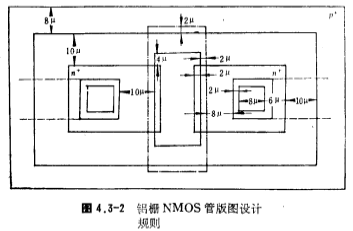
(4) The n-channel MOS tube must also be surrounded by a P+ diffusion area of 8 microns to prevent leakage between the n-channel MOS tube due to the field opening, as shown in Figure 4.3-2.
(6) The minimum distance between the P+ ring and the n+ drain-source region is 10 microns. This is because the registration accuracy between P+ and n+ lithography and the lateral diffusion of P+ and n+ are taken into consideration. Aluminum gate CMOS process design rules.
3. n+ lithography
The design rule of n+ lithography plate is basically the same as that of P+ lithography plate.
(1) The minimum width of the n+ zone is 8 microns.
(2) The minimum interval between n+ and n+ is 10 microns.
(3) The P area of the P-channel MOS tube must be surrounded by an n+ diffusion area of 8 microns, as shown in Figure 4.1-5a.
(4) The minimum distance between the n+ ring and the P+ missed area is 10 microns.
4. Grid pre-engraved hole lithography plate
(1) The gate area overlaps the drain-source area by 2 microns (minimum and maximum). In order to ensure that the channel area between the drain and source is covered by a thin gate oxide layer and has a certain lithography registration accuracy, the gate area must Overlap with the drain-source region, there is a certain lateral width due to the drain-source diffusion. Aluminum gate CMOS process design rules. Therefore, the amount of overlap does not need to be too large, otherwise the gate-source and gate-drain parasitic capacitances will increase.
(2) In the P channel width direction, in order to ensure the channel width W of the tube (determined by the width of the drain-source region), the gate region must extend beyond the drain-source region by at least 4 microns, as shown in Figure 4.3-2, generally In this case, the gate region can extend to the isolation ring.
(3) The pre-engraved lead hole plate is 2 microns larger than the lead hole plate.
(4) The minimum distance between the pre-engraved hole and the gate area is 10 microns to ensure the distance between the aluminum strip on the lead hole and the aluminum strip on the grid.
5. Lead hole lithography
(1) The minimum lead hole area is 8 microns × 8 microns or 6 microns × 10 microns.
(2) The minimum distance between the lead hole and the boundary of the drain-source diffusion region is 6 microns.
6. Aluminum strip lithography
(1) When the aluminum strip covers the lead hole, it protrudes at least 2 microns.
(2) When the aluminum strip covers the gate area in the channel length direction, it extends at least 2 microns,
(3) In the channel width direction, the aluminum strip on the gate area must extend to the isolation ring, and the overlap with the isolation ring is a minimum of 2 microns to prevent leakage in the edge area of the drain-source area. Aluminum gate CMOS process design rules.
(4) When the length of the aluminum bar is shorter than 250 microns, the minimum width of the aluminum bar is 8 microns, and the minimum interval between the aluminum bars is 8 microns.
(5) When the length of the aluminum bar is greater than 250 microns, the minimum width of the aluminum bar is 10 microns, and the minimum interval between the aluminum bars is also 10 microns.
(6) The minimum pressure point area is 120 microns × 140 microns.
(7) The minimum distance between pressure points is 120 microns.
(8) The minimum distance between the pressing point in the circuit and the aluminum bar is 40 microns.
Contact: Mr. Zou
Contact number: 0755-83888366-8022
Mobile phone: 18123972950
QQ: 2880195519
Contact Address: 5C1, Block CD, Tianji Building, Tianan Digital City, Chegongmiao, Futian District, Shenzhen
Please search WeChat official account: "KIA Semiconductor" or scan the following picture to "Follow" official WeChat official account
Please "follow" the official WeChat account: provide MOS tube technical assistance


