Electronic Technology Forum
Introduction to the typical circuit diagram of NMOS op amp (enhanced-depletion type) analysis
1. Fully enhanced NMOS operational amplifier
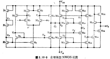
The fully enhanced NMOS operational amplifier is shown in Figure 3.10-9.
 form the input stage differential circuit, the gain is about 5 times;
 and
and it is a level shift circuit with a gain of about 0.95 times;
 the cascade amplifier and the output stage drive circuit are formed. The cascade amplifier is used to reduce the Miller capacitance of the M20 grid to improve the frequency response. The gain of this stage is equal to
 ,About 11 times;
 Form the output stage circuit, its form is shown in Figure 3.10-6, the gain is 6.6 times. In summary, the total gain of the circuit is about 345 times. M1, M2, M3 and M15, M16, M17 constitute a bias circuit, which determines the operating point of the circuit. M13 and
 compose the phase compensation circuit.
To make the circuit work normally, all MOS devices in the circuit are in the saturation zone. In order to achieve this requirement, the width to length ratio of each tube should have the following relationship (for simplicity, the tube width to length ratio is set as S).
We make ,so
,so , So I1/2 current flows through
 , The relationship is
 ,therefore
 have
have ,Select

have to as well as
 ,therefore
 Work in the saturation zone.
In M15, M16, M17 voltage divider circuit, select S16, S17, and use to make
 Working in the saturation zone, there should be
 . Operating points VA, VB and VC are shown in the figure. When designing, the current flowing through M1, M2 and M3 is 100 microamperes, VA=8V, VB=-11.5V, Vc=-7V, take MOS tube The threshold voltage VT=2 volts. The width and length ratio of each MOS device in the figure is shown in Table 3.10-1.
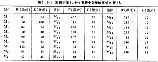
The main parameters of this circuit are shown in Table 3.10-2.

2. Enhanced-depletion NMOS operational amplifier
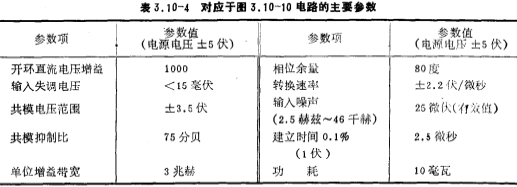
Figure 3.10-10 is an NMOS operational amplifier used in LSIMOS analog integrated circuits. It is made with a standard n-channel silicon gate enhancement-depletion MOS process. This op amp provides better performance. Typical circuit diagram of NMOS op amp. The open-loop DC gain is about 1000, and the common-mode rejection ratio is about 75 decibels. For a load of 1 kiloohm, the effective value of the output voltage can reach 1 volt (± 5 volts power supply voltage). When the capacitive load is 20 picofarads and the output amplitude is 1 volt, the settling time of 1% accuracy is about 2 microseconds.
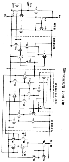
The ground is composed of input stage, level shift stage (including double-ended-single-ended conversion circuit), second gain stage and output stage. The output stage here is a negative feedback circuit with unity voltage gain. So from the perspective of gain, the circuit is composed of two gain stages. This is the same as the case of general-purpose op amps.
(1) Circuit description
The structure diagram of the input stage and level shift stage of the circuit is shown in Figure 310-11. They constitute a transconductance amplifier. The input stage is composed of M1~M7. M3 and M4 are depletion type active loads. Typical circuit diagram of NMOS op amp. M6 and M7 are the bias circuits of the input stage. M5 and M6 are current sources, and their current is determined by the bias circuit formed by M7 and M8. The input stage of this operational amplifier adopts the form of double-ended output, and other circuits have better common-mode rejection performance.
The level shift stage of this op amp is of low impedance type, and its specific circuit is composed of image.png in Figure 3.10-10. For the sake of discussion, draw this part of the circuit in Figure 3.10-12. In the figure, M11, M13 and M12, M14 respectively form parallel feedback, etc.
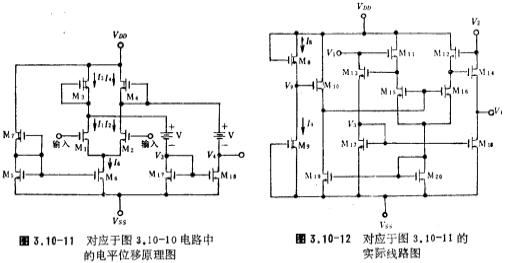
For effect diodes, the drain-source voltages of M13 and M14 are the voltages required for level shifting, that is, the battery voltage V in Figure 3.10-11. The M17 and M18 connected to their sources constitute a current source circuit to achieve the first-level output. The double-ended to single-ended conversion of current. The M15 and M16 pairs provide two equivalent diode currents respectively. This current is equivalent to the current source Io in Figure 3.10-5a, while the currents of M15 and M16 are biased by M20. M19 and M20 are another current source circuit, and the current of M10 biasing M20 is determined by M10. M8 and M9 form the total bias circuit of this stage. The structure of the bias circuit in this level shift stage is complicated, and its purpose is to make the gate voltages of M11 and M12 equal to Vo. Typical circuit diagram of NMOS op amp. It can be seen from Figure 3.10-12 that V1 and V2 are the drain voltages of the input stage differential pair transistors M1 and M2. The magnitude of this voltage directly determines the positive common-mode input voltage range of the op amp. In order to increase the common-mode voltage range, the voltages V1 and V2 should be as close as possible to the positive power supply voltage. Here, the conditions for M3 and M4 to enter the linear region are

In Figure 3.10-10 (see Figure 3.10-11 and Figure 3.10-12), the purpose of the entire bias circuit is to make

To ensure that the circuit has the largest common-mode input voltage range, It is biased by M8 and M9. The figure shows:
 The question now is how to make V1, V2 and V3 equal.
When designing the circuit in Figure 3.10-10, make the M10, M11, and M12 channels have the same width-to-length ratio. The design values of the width-to-length ratio of the current sources M19 and M20 meet:

Therefore, the current of M20 is twice the current of M19 (ie, M10). M15 and M16 are pairs of tubes. The current in M15 (M11) and the current in M10 (M12) are equal to the current in M10. As a result, M10, M11, and M12 must have the same VGS. The width-to-length ratio of M10, M11, and M12 channels are all designed to be less than 1, and The aspect ratio is very large, so the gate-source voltage of the former is much larger than that of the latter. Therefore, the drain voltage of M15 and M16 can be approximated as
 The drain voltages are equal. It can be seen that V1, V2 and V0 are approximately equal. AC equivalent resistance of the above equivalent diode
 it is about 6 kiloohms here.
The second gain stage of the op amp is composed of M21~M24, and the current injection method is used to increase the transconductance of the amplifier tube M21, thereby increasing the gain of the second stage. The circuit form is exactly the same as in Figure 3.10-1b. The capacitor C in the circuit is used for frequency compensation.
The output stage of the op amp is determined by
Composition, and its circuit form is the same as Figure 3.10-8. It works in Class A and B status, and its output stage output resistance is about 800 ohms.
The frequency characteristic of this op amp mainly depends on the second stage. The Miller compensation capacitor C determines the main pole of the circuit. Its design value is 8 picofarads. In order to reduce the feedforward influence of the capacitor C and increase the gain of the second stage, the transconductance of M21 should be increased as much as possible in the circuit design. In the circuit, use and the zero generated by the capacitor C to compensate the second pole of the circuit to improve the amplitude-frequency characteristics and phase margin of the entire circuit at high frequencies.
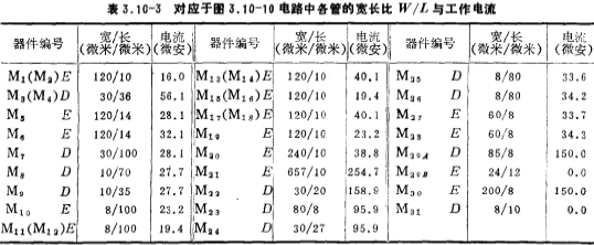
The size design value and current value of each device of this operational amplifier circuit are shown in Table 3.10-3. Among them, the width and length of the M3 and M4 channels are both larger, which is considered from reducing the 1/f noise of the op amp. In the table, E is an enhanced device, and D is a depletion device. The circuit is made using NMOS silicon gate technology, and the main parameter values of the circuit are shown in Table 3.10-4.
The NMOS operational amplifier discussed above has a low voltage gain. In recent years, high-performance, high-gain NMOS operational amplifiers have been developed with a voltage gain of 40,000 times.
Contact: Mr. Zou
Contact number: 0755-83888366-8022
Mobile phone: 18123972950
QQ: 2880195519
Contact Address: 5C1, Block CD, Tianji Building, Tianan Digital City, Chegongmiao, Futian District, Shenzhen
Please search WeChat official account: "KIA Semiconductor" or scan the following picture to "Follow" official WeChat official account
Please "follow" the official WeChat account: provide MOS tube technical assistance


