Electronic Technology Forum
Detailed analysis of the schematic diagram of NMOS single-stage amplifier and low impedance level shift
In terms of circuit performance, a single-channel NMOS op amp is worse than a CMOS op amp because it lacks complementary devices and the circuit form is more complicated. However, since the speed and integration of NMOS circuits are higher than those of CMOS circuits, it is very attractive in LSIMOS analog integrated circuits. Especially when a charge conversion device is included in the MOS analog circuit, it is usually realized by an NMOS process. In fact, the first all-MOS op amp circuit is an NMOS op amp. Compared with CMOS operational amplifiers, NMOS operational amplifiers have the following differences:
(1) Compared with CMOS circuits, the single-stage common-source amplification or differential amplification of NMOS has lower gain. In order to improve the voltage gain of the NMOS amplifier, some special circuits are used to make the circuit structure more counter-stained.
(2) In order to ensure zero input and zero output, the NMOS operational amplifier must have a level shift circuit. The level shift of the CMOS operational amplifier is realized by the complementary performance of the device, and there is no special level shift circuit. From this point of view, the circuit structure of the NMOS operational amplifier is more complicated.
(3) In order to improve the output performance of the NMOS operational amplifier, the output stage circuit adopts a special circuit form, which is more complicated than the CMOS complementary output circuit.
(4) The DC level configuration of CMOS operational amplifiers is relatively simple, while the DC level configuration of NMOS operational amplifiers is more difficult. Therefore, when designing an NMOS operational amplifier, the setting of its operating point is very important.
The following first describes some special circuits in the NMOS operational amplifier, and then introduces two different types of NMOS operational amplifier.
1. NMOS single-stage amplifier
From the discussion in Chapter 2, we can see that the voltage gain of an NMOS amplifier with a depletion load is higher than that with an enhanced load. But even so, the voltage gain of an NMOS amplifier with a depletion load is still lower than that of a CMOS amplifier. In most cases, its gain value is about 30~100. From the perspective of circuit design, additional injection current and methods of increasing the transconductance of the amplifier tube can be used to increase the voltage gain of the depletion-type load NMOS amplifier.
The schematic circuit diagram of this scheme is shown in Figure 3.10-1a. M1 and M2 in the figure constitute a cascode series amplifier, M2 is an active load, and part of the leakage current of M1 is injected by the current source I. , The current flowing through M1 increases, and its transconductance increases. When the transconductance of M1 increases, the currents of M2 and M3 are not increased. At this time, M2 and M3 are still working in the saturation region, and their equivalent output resistance remains unchanged. Therefore, the multiplier that the transconductance of M1 increases determines the multiplier that the voltage gain of the amplifier increases.

3.10-1b is a specific circuit structure, in which the current source I is replaced by the depletion NMOS transistor M4 shorted by GS. Since the currents of M1 and M2 are different, the transconductance values are also different, so the voltage gain of the circuit is

Where SR is the ratio of the width to length ratio of M1 and M2 These are the drain currents of M1 and M2, respectively. Compared with the formula of Chapter 2 (2.4-10), the increase of gain is
 . In the E/DNMOS operational amplifier, the common source amplifier circuit usually adopts the circuit structure shown in Figure 3.10-1b to increase the operational amplifier gain.
2. Level shift circuit
(1) High impedance level shift circuit
Figure 3.10-2 is a high-impedance level shift circuit. While realizing the level shift, it also realizes the conversion from double-ended to single-ended. NMOS single-stage amplifier. M1 and M2 are source followers, and M3 and M4 are current source circuits. The impedance of the input end and the output end of this level shift circuit is very high. According to the equivalent circuit, the differential gain is less than 1.

When designing the operational amplifier circuit, in order to ensure sufficient voltage gain, it must include two gain stages. When a level shift stage is inserted between the two gain stages, since the output and input of the level shift stage are both high impedance characteristics, the operational amplifier circuit of this structure must contain three high impedances. node. That is, the input and output nodes of the level shift stage and the output node of the second gain stage. The more high-impedance nodes in the circuit, the more its poles, and the more difficult the phase compensation of the circuit. At this time, the phase margin of the circuit is reduced, and ringing or high-frequency oscillation may occur after the closed loop. This is a shortcoming of the high impedance level shift circuit.
(2) Low impedance level shift circuit
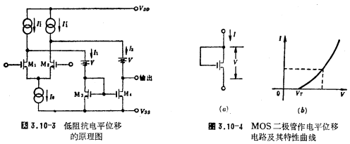
The characteristics of the low impedance level displacement stage is like a voltage source, which is equivalent to the battery V in Figure 3.10-3. In the figure, M3 and M4 are current source circuits, which realize double-ended-single-ended conversion. At this time, the output of the input stage is equivalent to a low-impedance node. From the perspective of the overall operational amplifier circuit, this level shift circuit facilitates phase compensation. The key here is to generate a floating voltage source, which can track the discrete changes of the power supply voltage and device parameters to ensure that the front-end circuit has a larger positive common-mode input voltage range and better power supply voltage suppression characteristics. The simplest level shift circuit to realize the above scheme is a MOS tube connected in the form of a diode, as shown in Figure 3.10-4a. NMOS single-stage amplifier. However, its characteristics are very unsatisfactory. In order to ensure a large enough voltage drop across the MOS tube, its aspect ratio must be designed to be small. Therefore, its output resistance is very large. Its characteristic curve is shown in Figure 3.10- Shown in 4b.

In order to obtain a low-impedance floating voltage source, a parallel feedback circuit as shown in Figure 3.10-5a can be used. In this circuit, when the voltage V exceeds the voltage , M2 is turned on. Here
  is
is

Io in the figure is a constant current source, it determines the M1 . It can be seen from the current-voltage relationship of the MOS tube,
 is
is

therefore

will

Substituting into the current relationship of M2, we can get

Putting the (3.10-2) style on behalf of others, then there are

The above formula shows that the circuit characteristic in Figure 3.10-5a is equivalent to an equivalent diode-connected MOS tube, but its threshold voltage is It is determined by the formula (3.10-4). Obviously, the output conductance of this circuit is

That is, its output conductance is the transconductance of the equivalent MOS tube. Since the output voltage V of the circuit is the sum of the GS voltages of M1 and M2, it does not require it is very large, so the aspect ratio of M2 can be designed to be larger, that is, its transconductance is larger, so its equivalent output resistance is very small, and the slope of the VI curve of the equivalent MOS diode is steep, as shown in Figure 3.10-5b As shown, the transconductance of M1 in this circuit is designed to be small to obtain a larger
 .
.
[Example] The parameters in the figure 3.10-5a are

 volts, and Io=20 microamperes, using the formula (3.10-4) to get

When V=9 volts, the output impedance from (3.10-6) is

3. Output stage circuit
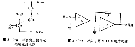
In the NMOS circuit, the output stage with low output impedance often uses a parallel negative feedback circuit, as shown in Figure 3.10-6. The output impedance of this circuit is low, and at the same time it has very good whisker rate characteristics. Therefore, it will not seriously affect its phase margin in the application of operational amplifiers. NMOS single-stage amplifier. In fact, the circuit can be seen as the structure of Figure 3.10-7. Among them, the first stage is a transimpedance amplifier, and the second stage is a transimpedance amplifier, so the total gain Av of the circuit is


In Figure 3.10-6, the transimpedance amplifier is formed by M1, and the transimpedance amplifier is formed by the negative feedback amplifiers of M2~M4.
According to the equivalent circuit, ignoring the substrate effect of the circuit, its voltage gain Av is

And the output resistance of the circuit is

The forward voltage swing of this circuit can reach , And the negative voltage swing is slightly smaller.
The output stage circuit shown in Figure 3.10-8 is an improved form of the circuit in Figure 3.10-6. It maintains the advantage of low output impedance, and changes from Class A amplification to Class A and B push-pull amplification, which enhances the output capacity. The voltage gain of is approximately 1.

The tube parameters of the circuit can be selected in this way, M1 and M2, M3 and M4 take the same aspect ratio, for example, take

In this way, under static conditions,
, So that the input voltage Vi is equal to the output voltage Vo. When Vi is a forward voltage, M6 tube electrical diagram 3.10-8 corresponds to Figure 3.10-6, the current increases, and at the same time, the drain voltage of M4 tube decreases due to the increase of current, that is, the improved form of the circuit M3 tube The grid potential of V decreases and the current of the M3 tube decreases, so that the output current increases, and a positive voltage is obtained on the load at the output end; when Vi is a negative voltage, the current of the M6 tube decreases, and the current of the M5 tube increases. A negative voltage is obtained on the load resistance of the output terminal. Therefore, the circuit in Figure 3.10-8 is a Class A and Class B push-pull output stage circuit.
Contact: Mr. Zou
Contact number: 0755-83888366-8022
Mobile phone: 18123972950
QQ: 2880195519
Contact Address: 5C1, Block CD, Tianji Building, Tianan Digital City, Chegongmiao, Futian District, Shenzhen
Please search WeChat official account: "KIA Semiconductor" or scan the following picture to "Follow" official WeChat official account
Please "follow" the official WeChat account: provide MOS tube technical assistance


