Electronic Technology Forum
CMOS voltage comparator with automatic offset compensation and its working principle
In order to improve the sensitivity of the CMOS voltage comparator, the offset auto-zeroing technique introduced in the previous section can be used. The circuit form is shown in Figure 3.9-3. This circuit is similar to the circuit in Figure 3.8-5 in Section 8 of this chapter. The principle of zero adjustment has been explained. The circuit in Figure 3.9-3 is a low-offset voltage comparator circuit. The following briefly introduces the working principle of the CMOS voltage comparator. In the figure, VR is the reference voltage, and Vi>VR is the input signal voltage. The working state of the circuit can be controlled by a bi-phase clock signal. In the first working state, when the switch S1 is closed and S2 is open, the voltage comparator is in a zero-potential output state, and the reference voltage VR charges the capacitor C, so that the VR voltage is registered on the capacitor C, which is two parts of the capacitor C. The voltage at the terminal Vc=VR; in the second working state, when the switch S1 is opened and S2 is closed, the circuit enters the comparison state, and the voltage comparator is in the amplification state. Because the capacitor C loses the charging circuit (the amplifier input impedance is very high), The charge at both ends of the capacitor C cannot change, so the potential V- of the inverting input terminal of the amplifier is Vi>VR, and the output voltage Vo is


As long as A is large enough and Vi>VR, Vo is low level; when Vi>VR, Vo is high level, thus completing the function of comparing the input signal Vi with the reference voltage VR. In order to increase the gain of the voltage comparator, the CMOS voltage comparator can use the circuit structure shown in Figure 3.9-4, and its gain is A1A2.
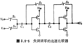
In order to obtain a low-offset, high-speed voltage comparator circuit, the A1 and A2 amplifiers in Figure 3.9-4 use high-speed, simple-structured CMOS inverter amplifiers, and the circuit form is shown in Figure 3.9-5. It is used in high-speed analog-to-digital converters.

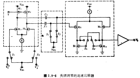
Another high-speed voltage comparator is shown in Figure 3.9-6. It consists of three parts:
1. High-speed pre-differential amplifier (M1~M4);
2. The switches (S1~S2) and capacitors (C1, C2) of the offset voltage elimination circuit;
3. Positive feedback amplifier circuit (M5~M8). The circuit is divided into two working states. In the first working state, the switch S1S2 short-circuits the input terminal and the surface S3S4 is turned on. At this time, the input stage offset voltage is registered on the capacitors C1 and C2; CMOS voltage comparator; the second working state , Switches S1 and S2 are respectively connected to the input signal, switches S3, S4 are off, M5~M8 constitute a positive feedback amplifier, at this time the offset voltage has been eliminated, and the input signal is amplified by the input stage to the positive feedback amplifier (M5~M8) Compare, output high level or low level after comparison.

Contact: Mr. Zou
Contact number: 0755-83888366-8022
Mobile phone: 18123972950
QQ: 2880195519
Contact Address: 5C1, Block CD, Tianji Building, Tianan Digital City, Chegongmiao, Futian District, Shenzhen
Please search WeChat official account: "KIA Semiconductor" or scan the following picture to "Follow" official WeChat official account
Please "follow" the official WeChat account: provide MOS tube technical assistance


