Electronic Technology Forum
The working principle of CMOS voltage comparator and the main characteristics of the circuit
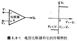
The voltage comparator is basically the same as the op amp in terms of circuit structure, electrical performance, etc., and its symbol representation is exactly the same as that of the op amp, that is, there are two input terminals, in-phase and reverse phase, and one output terminal. The open-loop gain is denoted by A. The function of the voltage comparator is to compare the magnitude of the two analog input signals and get a high level or a low level at the output. If V+, and V- are used to denote the voltage at the non-inverting input terminal and the inverting input terminal respectively, then for an ideal voltage comparator, its characteristic can be expressed as: when V+ is greater than V-, its output is high; when V -When it is greater than V+, its output is low. Figure 3.9-1a and b respectively show the symbol of the voltage comparator and the transfer characteristics of the ideal voltage comparator.

In fact, when the output terminal of the voltage comparator changes from low level to high level, or from high level to low level, it takes a certain amount of time (determines the transient response of the voltage comparator), and secondly, due to the voltage comparator The gain of is limited, and there is an offset voltage, so there will be an uncertain voltage at its input, which will directly affect the sensitivity of the voltage comparator (the sensitivity of the input voltage discrimination). The higher the open-loop gain A of the voltage comparator, the smaller the offset voltage, and the smaller the uncertainty voltage, that is, the higher the sensitivity. For a high-performance voltage comparator, it should have a high open-loop gain A, a low offset voltage and a high slew rate. Obviously, general operational amplifiers can also be used as voltage comparators. However, in the design of the operational amplifier circuit, the linear transmission characteristics between the output and the input and the stability of the frequency compensation are emphasized. Therefore, the response time and delay time of the operational amplifier are often very large, and the open-loop gain is not very high. If a high-speed or high-sensitivity voltage comparator is required, it is usually not appropriate to use an operational amplifier instead. We can design the voltage comparator according to the requirements. When designing the voltage comparator, the design principle of its DC characteristic is basically the same as that of the op amp circuit, while the design of the frequency characteristic is different from that of the op amp circuit. Generally, the voltage comparator works under open-loop conditions, so there is no need to consider the frequency compensation of the amplifier's closed-loop stable operation within the circuit. Since the inherent shortcoming of the MOS type differential amplifier is that its input offset voltage is relatively large, when it is used to directly construct the voltage comparator circuit, the input uncertainty area of the comparator is very large, and the sensitivity of the comparator is reduced. Therefore, in the MOS voltage comparison Attention should be paid to reducing its input offset voltage when designing the circuit of the device.
The integrated voltage comparator, like the integrated operational amplifier, has a wide range of uses. The voltage comparator is an indispensable main component in analog integrated circuits such as analog-to-digital converters. Using CMOS technology, using the various unit circuits introduced in Chapter 2 and the offset voltage auto-zeroing technology in the previous section of this chapter, a voltage comparator with better performance can be designed. This section introduces several design methods of CMOS voltage comparators.
1. Working principle of CMOS voltage comparator
The circuit shown in Figure 3.9-2 is a schematic diagram of the CMOS voltage comparator 5G14574 circuit.
Compared with the commonly used two-stage op amp, the 5G14574 voltage comparator adds a two-stage inverter and removes the internal compensation capacitor. As can be seen from the figure, it is a four-level zoom. The first stage is a differential input stage, which converts double-ended to single-ended output, and two n-channel MOS tubes as current source loads. In addition to increasing the gain of the second stage, it is also designed to ensure that its output voltage is at the midpoint of the power supply voltage in a static state to ensure that the subsequent CMOS inverter is biased in the high gain area. The third and fourth stages are CMOS inverters biased in the high gain region. According to the circuit parameters and process parameters and through actual testing, the open loop gain A of this circuit is about 100,000 to 200,000 times.
The 5G14574 voltage comparator includes four full MOS voltage comparators with the same unit, referred to as four comparators, and its bias current image.png is determined by the external bias resistor image.png. The magnitude of the bias current will directly affect the rise time and delay time of the circuit. Increasing the bias current can speed up the rise time and shorten the delay time, but the power consumption of the circuit increases.
When this circuit is in use, usually one end of the differential input stage is connected to the reference voltage VR, and the other end is connected to the measured voltage image.png; according to the requirements of the output polarity, image.png is connected to the non-inverting input or the inverting input. When image.png or image.png, the output state is reversed. In principle, if there is no voltage offset, according to the voltage gain of this circuit, its sensitivity can reach 50-100 microvolts. Since the circuit itself has an offset voltage that drifts with time and temperature, the offset voltage is about ±10 millivolts. Therefore, it is very difficult to detect weak signals below millivolts.
2. Main features of CMOS circuit
According to the circuit structure, the main features of the CMOS voltage comparator 5G14574 are:
(1) Compatible with CMOS logic circuits, without level conversion.
(2) Low power consumption, bias current at microamperes, the total quiescent current of the four comparators is only 100 microamps.
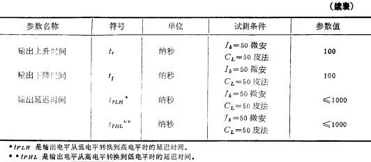
(3) High slew rate, at VDD=10V, when CL=50 picofarads, the rise time tr and the fall time tr are approximately 100 nanoseconds, and the slew rate is 100 volts/microsecond at this time.
(4) The input impedance is high, generally greater than 10° ohms.
(5) As the CMOS inverter is used as the output stage, it can achieve full amplitude output, high level VOH=VDD, low level VOL=VSS.
(6) Both single and dual power supplies can work.
(7) External bias resistor RD, bias current can be flexibly set.
(8) The offset voltage is large, usually about 10 millivolts. If you need to detect small signals below millivolts, you must take compensation measures. According to the size and polarity of the circuit offset voltage Vos, a Vos voltage can be deducted from the reference voltage in advance .
The main parameters of the 5G14574 voltage comparator are shown in Table 3.9-1.


Contact: Mr. Zou
Contact number: 0755-83888366-8022
Mobile phone: 18123972950
QQ: 2880195519
Contact Address: 5C1, Block CD, Tianji Building, Tianan Digital City, Chegongmiao, Futian District, Shenzhen
Please search WeChat official account: "KIA Semiconductor" or scan the following picture to "Follow" official WeChat official account
Please "follow" the official WeChat account: provide MOS tube technical assistance


