Electronic Technology Forum
Technical method of automatic zero adjustment of MOS operational amplifier and switched capacitor circuit
1. The general method of automatic zero adjustment
In MOS analog large-scale integrated circuits, as the main component of the MOS operational amplifier, the simpler the circuit structure, the better, in order to reduce the chip area; but the general MOS operational amplifier has a relatively large offset voltage, about 10-20 milliseconds Volt, which limits its scope of use. In order to reduce the offset and drift of the general structure of the MOS operational amplifier, we can adopt the automatic zero adjustment technology that is easy to integrate, which is described in detail as follows.
The circuit in Figure 3.8-3 is the schematic diagram of the MOS amplifier circuit with the offset voltage automatically zeroed. Amplifier A is a MOS amplifier with differential input and differential output. Switches S1~S4 are analog switches composed of MOS devices. Capacitors It is used to register the offset current of the amplifier. The circuit works in two stages. In the first stage, switches S1~S4 are closed, the input is zero, and the output voltage (ie, the offset voltage) is stored in the capacitor.
 and
and above, this stage is called the offset zero stage; in the second stage, the switches S1~S4 are disconnected, and the input signal is amplified by A and output at the output terminal. If the impedance of the output terminal is very high, it is stored in the capacitor
 the offset voltage on the upper side continues to be maintained, and the signal at the output end is only the signal amplified by the input signal, which eliminates the offset voltage of the amplifier. This stage is called the measurement stage. The automatic zero adjustment of the MOS operational amplifier; the above two stages are controlled by the beat pulse respectively.
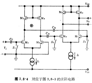
The two-stage MOS differential amplifier with auto-zeroing technology is shown in Figure 3.8-4.

When the switches S1~S2 are closed, the offset voltage output by the first-stage differential amplifier is registered in the capacitor at this time, the output voltage of the second stage is only the offset voltage of the second stage; when the switches S1~S2 are off, the input signal is amplified by the first stage and the second stage to the output terminal, because this stage is stored in the capacitor
 the offset voltage on the upper side remains unchanged, so that the offset voltage of the first-stage differential amplifier does not affect the second-stage differential amplifier, that is, the municipal offset voltage is eliminated, so that the total offset of the second-stage differential amplifier is greatly reduced. Suppose the gain of the first stage is
A1, the offset voltage is Vos1, the second stage gain is A2, the offset voltage is Vos2, then the output voltage Vo can be written as

It can be seen from the above formula that the offset voltage Vos equivalent to the input terminal is

Obviously, the offset voltage of the amplifier is to reduce the offset voltage of the second stage by a factor of A1. Increase the gain A1 of the first stage to reduce the offset voltage of the amplifier.
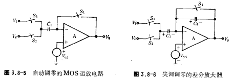
Figure 3.8-5 shows the MOS operational amplifier circuit with automatic zero adjustment. The voltage at the forward input terminal of the operational amplifier in the picture is the offset voltage of the operational amplifier. When S1 is closed and S2 is disconnected, the voltage across capacitor C1 is V1-Vos; the MOS operational amplifier is automatically zeroed; when S1 is disconnected and S2 is closed, the input signal voltage V1 becomes V2, and the two ends of capacitor C1 The voltage cannot be changed, so the voltage at the negative input of the op amp is V2-V1+Vos, which can be obtained according to the relationship between the input and output of the op amp.

The above formula shows that the output voltage of the op amp has nothing to do with the offset voltage, only the difference of the input signal, so the circuit in Figure 3.8-5 is a differential amplifier with automatic zero adjustment. It can be seen from the figure that if the V1 input terminal is grounded, an inverted phase amplification is formed; if the V2 input terminal is grounded, an in-phase amplification is formed. Usually the circuit shown in Figure 3.8-5 can be used as a comparator.
2. Using the zero adjustment technology of switched capacitor circuit
In recent years, switched capacitor circuits composed of MOS operational amplifiers, MOS switches and MOS capacitors have developed rapidly and have become one of the main circuit forms of today's MOS large-scale analog integrated circuits. The switch response circuit can use the offset auto-zeroing technology to form various amplifiers, comparators and integrators with low offset.
The circuit in Figure 3.8-6 is a closed-loop differential amplifier with offset zero adjustment, and its working principle is as follows:

When switch S1 is closed and S2 is open, the voltage across capacitor C1 is Vc1=V1-Vos; when switch S1 is open and S2 is closed, the voltage across capacitor C1 changes from V1-Vos to V2-Vos, and capacitor C2 The voltage across both ends is image.pngimage.pngAccording to the principle of conservation of charge, the following charge equation is obtained:

The above formula is sorted out

The above formula shows that the gain is determined by the ratio of C1 and C2. In order to obtain a certain gain, the ratio of C1 and C2 can be selected. Dividing the offset voltage Vos of the op amp by C1 and C2 is the offset voltage of the amplifier.
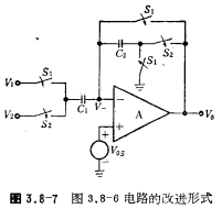
The disadvantage of the circuit in Figure 3.8-6 is that the offset voltage cannot be completely eliminated. In order to overcome this shortcoming, some improvements can be made on the basis of Figure 3.8-6 to eliminate all the offset voltage. The circuit form is shown in Figure 3.8-7. Show. The working principle is briefly described as follows.

When switch S1 is closed and switch S2 is open, the voltage across capacitor C1 , The voltage across capacitor C2
 ; Automatic zero adjustment of MOS operational amplifier; when switch S1 is open and S2 is closed, the voltage across capacitor C1
 From V1-Vos to V2-Vos, the voltage Vc across the capacitor C2 is determined by
 Change to Vos-Vo. According to the principle of conservation of charge, the following charge equation can be obtained:

Organize the above formula into

The formula (3.8-12) shows that the output voltage has nothing to do with the offset voltage of the op amp.
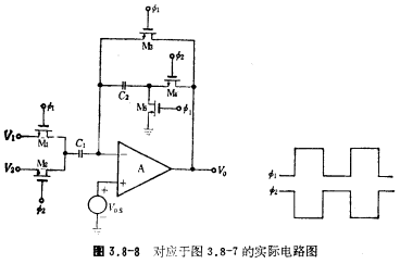
Because the circuit in Figure 3.8-7 eliminates the offset, its offset zeroing method is widely used in switched capacitor circuits. The switches in the picture are usually composed of MOS switches, and the actual circuit is shown in Figure 3.8-8. The n-channel MOS tube in the figure constitutes an analog switch. ф1 and ф2 are bi-phase clock signals. When ф1 is high (ф2 is low), M1, M3, and M5 are on, M2 and M4 are off: when ф2 is high When level (ф1 is low level) M2, M4 are on, M1, M3 and M5 are off.

Contact: Mr. Zou
Contact number: 0755-83888366-8022
Mobile phone: 18123972950
QQ: 2880195519
Contact Address: 5C1, Block CD, Tianji Building, Tianan Digital City, Chegongmiao, Futian District, Shenzhen
Please search WeChat official account: "KIA Semiconductor" or scan the following picture to "Follow" official WeChat official account
Please "follow" the official WeChat account: provide MOS tube technical assistance


