Electronic Technology Forum
CMOS operational amplifier ICL7650 working principle diagram and output voltage relationship analysis
The working principle of dynamic zero CMOS operational amplifier ICL7650
For a long time, integrated circuit designers have made unremitting efforts in process technology and circuit design, trying to solve the problems of misalignment and drift of integrated op amps. Generally, the offset and drift of MOS integrated operational amplifiers are larger than those of bipolar integrated operational amplifiers; however, after reasonable circuit design and layout design, and the use of new processes (such as ion implantation processes), MOS integrated operational amplifiers can be integrated The offset is controlled within 10 millivolts, reaching the level of a bipolar integrated operational amplifier. However, this MOS integrated operational amplifier still has some problems as weak signal amplification, high-precision measurement amplification, integrator and high-resolution comparator, etc. The main reason is the offset and drift of this MOS integrated operational amplifier. For this reason, people are committed to researching amplifiers with good DC characteristics. In the early 1980s, Intersil Corporation of the United States developed a dynamic zero CMOS operational amplifier ICL7650 designed with full MOS technology, with an offset of 0.01 microvolts, a temperature drift of 0.01 microvolts/℃, an open loop gain of 130 dB, and a common mode rejection ratio. It is 130 decibels. It can be said that the dynamic zero-calibration CMOS op amp ICL7650 is close to the "ideal" op amp in terms of DC characteristics, which makes the integrated op amp enter the fourth generation and establishes the importance of MOS op amp in analog integrated circuits. status. This section will introduce the design idea of the dynamic zero CMOS integrated operational amplifier ICL7650, and give the circuit structure, at the same time will introduce the offset voltage automatic zero calibration technology currently used in the low offset MOS integrated operational amplifier.
The design idea of ICL7650 is actually to absorb the advantages of low offset and low temperature drift of the traditional dual-channel amplifier, while improving the circuit structure to overcome the shortcomings of the traditional circuit and make the circuit suitable for monolithic integration. The core of this so-called fourth-generation operational amplifier design concept is to use clock pulses to control the entire circuit to make it work in two stages. The first stage is amplifier error detection and registration, and the second stage is zero calibration and amplification. So as to achieve low offset and low temperature drift.
1. The working principle of ICL7650
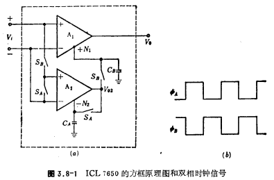
Figure 3.8-1a shows the block diagram of ICL7650.

A1 is the main amplifier, which is used to amplify the input signal and output the amplified signal. This amplifier has a wider frequency band and a stronger load capacity. A1 not only has two non-inverting and inverting input terminals like ordinary op amps; it also has a third input terminal N1, which has the same function as the non-inverting input terminal. If a signal is added from N1, the output terminal will be A1 amplified in-phase signal.
A2 is a zero-adjusting amplifier; it is used to reduce the offset voltage of the main amplifier A1, and does not directly output signals to the outside, and is only used as an auxiliary amplifier. In addition to the two input terminals of ordinary op amps, this circuit also has a third input terminal N2 like A1. N2 is an inverting input terminal, that is, the signal added by N2 is amplified by A2 and appears inverted at the output terminal of A2.
The switches SA and SB are analog switches composed of MOS devices, which are controlled by a two-phase clock signal (Figure 3.8-1b). If the double-ended clock signal is divided into A phase and B phase clock signals, when the A phase is high, the switch SA is on and the switch SB is off; when the B phase is high, the switch SB is on and the switch SA is off . The clock signal is generated inside the circuit and can also be added from outside.
CA and CB are external capacitors, which play a role in registering the offset voltage. Now we briefly introduce the working principle of the circuit in Figure 3.8-1a.
When the phase A of the bi-phase clock signal is at a high level, the switch SA is closed and the switch SB is open. It can be seen from the figure that at this stage (called the first stage), the input of A2 is closed, and its output voltage is only related to the offset voltage of A2. The third input terminal N2 is directly connected to the output for full feedback. At this time, the capacitor CA registers the offset voltage of the A2 amplifier. When the B phase of the bi-phase clock signal is at a high level, the switch SB is closed and the switch SA is opened, and this is the second working phase. As can be seen from the figure, the input signal is connected to the differential input of A2 Due to the existence of the offset voltage of the A2 amplifier, it is amplified together with the input signal and sent to the output terminal of A2: At the same time, the offset voltage of A2 registered by the capacitor CA is also amplified through the third input terminal N2. Since the contribution of the equivalent offset voltage of the differential input terminal of A2 to the output terminal is exactly the same as the contribution of the offset voltage of A2 at the N2 terminal to the output terminal (equal magnitude and opposite polarity), the signal at the output terminal of A2 is only the same as the input signal
 it has nothing to do with the offset voltage of A2, that is to say, due to the work result of the first stage, the output of A2 has no offset voltage component in the second stage, that is, the offset has been adjusted to zero.
Look at the working condition of amplifier A1. At this time, A1 not only amplifies the input signal of the differential input terminal, but also amplifies the offset voltage of A1; at the same time, the signal from the output terminal of A2 is added to the terminal N1 of the amplifier A1, so the output terminal of A1 gets three parts Signal, two of which are related to the input signal, and one is related to the offset voltage of A1. The component related to the input signal image.png is greater than the offset voltage component, which greatly reduces the offset voltage of the amplifier.
2. The relationship between the output voltage of ICL7650 and the input signal and offset voltage
To facilitate analysis, we make the following four assumptions:
(1) Ao1 and Ao2 are the amplification factors of the main amplifier A1 and the zero-adjusting amplifier A2 respectively (from the differential input terminal to the output terminal);
(2) Ao'1 and Ao'2 are the magnifications of amplifiers A1 and A2 when N1 and N2 are used as input terminals, respectively;
(3) respectively are the equivalent offset voltages of A1 and A2 at the input;
(4) The influence of the common mode rejection ratio (CMRR) on the amplifier is not considered for the time being.
The first phase of the clock; switch SA is closed, switch SB is open, and the input voltage of the zero-adjusting amplifier A2 is  . At this time, the output voltage Vo2 of A2 is expressed by the following formula:

Simplified

At this time, the output voltage Vo2 of A2 is all registered in the capacitor CA, that is, the voltage VCA of the capacitor CA is

The second phase of the clock: switch SB is closed, switch SA is open, input signal divided into two channels for amplification, one part is input from the input of A1 for amplification, which also means that A1 is continuously amplifying the input signal, and the other part of the input signal is added to A2 for amplification. At this time, the output voltage of A2 is V0'2 Is given by:

Since SA is disconnected, the offset voltage Vos charged into the capacitor CA in the first half cycle enters A2 from the zero-adjusting input terminal N2 for amplification, and the output voltage V0′2′ of this part is

The contribution of the above two parts of output voltage at the output of A2 is

The output voltage of the above A2 is registered in the capacitor CB, and is also added to the non-inverting input terminal N1 of A1 for amplification. At this time, the output voltage Vo of the main amplifier A1 can be expressed as

In the formula (A01+A′01A02) is the gain of the entire amplifier, and A01Vos is the error term of the offset voltage, which is referred to the offset voltage Vos of the input terminal as

Since A01~A'01,

It can be seen from the above formula that the offset voltage VDS of the circuit reduces the offset voltage of the A1 amplifier by A02 times. As long as the zero-adjusting amplifier A2 has a sufficiently large gain, the offset voltage Vos is very small. For example: Vos, which is 10 millivolts, and the gain of the zero-adjusting amplifier A02=10000 times, the offset voltage Vos is only 1 microvolt.
It can be seen from the formula (3.8-6) that the open loop voltage gain of the circuit is very high, reaching about 130 decibels.
If the influence of the common-mode rejection ratio is considered, then, through calculation, the common-mode rejection ratio of the circuit in Figure 3.8-1a is

Where CMRR1 is the common-mode rejection ratio of the A1 amplifier.
Therefore, the common-mode rejection ratio of the circuit in Figure 3.8-1a is Ao2 times the common-mode rejection ratio of the A1 amplifier. If CMRR1=60 decibels and A02=70 decibels, the common-mode rejection ratio CMRR of the circuit is 130 decibels.
In summary, the ICL7650 integrated operational amplifier is a high-performance operational amplifier with high gain, high common-mode rejection ratio, low offset and low drift.
3. The specific circuit of the amplifier in ICL7650
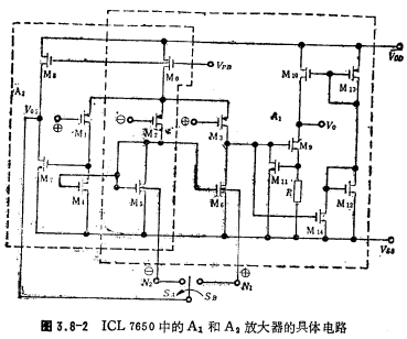
The A1 and A2 amplifiers in the circuit of Fig. 3.8-1a, the specific circuit is shown in Fig. 3.8-2.

The zero-adjusting amplifier A2 is composed of M1, M2, M4, M5, M7, and M8. Among them, M1 and M2 are the input stage differential pair tubes, M4 and M5 are the active loads of the differential amplifier, and M7 and M8 are the output stage circuits. The main amplifier A1 is composed of M2, M3, M5, M6 and M9~M14. Among them, M2 and M3 are input stage differential pair tubes, M5 and M6 are active loads of M2 and M3, and M9~M14 push-pull output stage circuits. It can be seen from the figure that the gate of M2 serves as the inverting input shared by the two amplifiers.
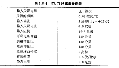
It can be seen from the figure that the N2 input terminal of the zero-adjusting amplifier A2 is the substrate (back gate) of M6, and the substrate potential is usually connected to the source or lower than the source voltage. Here, the substrate of M5 is floating. As the control gate, its voltage is slightly higher than the source voltage. When a positive voltage is input to the N2 terminal, due to the substrate modulation effect, the threshold voltage of the M5 tube is reduced. Because the current of M5 remains unchanged, the VGS voltage of M5 decreases and the current of M4 decreases, thereby increasing the current of M7 , The output V02 drops, so N2 belongs to the inverting input. The N1 end of the main amplifier A1 is the substrate (back gate) of M6. The same analysis shows that N1 is the non-inverting input terminal. He pointed out that using the substrate as the control gate is a relatively novel design method of the ICL7650, which simplifies the circuit structure. The main parameters of ICL7650 are shown in Table 3.8-1.

Contact: Mr. Zou
Contact number: 0755-83888366-8022
Mobile phone: 18123972950
QQ: 2880195519
Contact Address: 5C1, Block CD, Tianji Building, Tianan Digital City, Chegongmiao, Futian District, Shenzhen
Please search WeChat official account: "KIA Semiconductor" or scan the following picture to "Follow" official WeChat official account
Please "follow" the official WeChat account: provide MOS tube technical assistance


