Electronic Technology Forum
Overview of the main parameters of high-performance CMOS power operational amplifiers
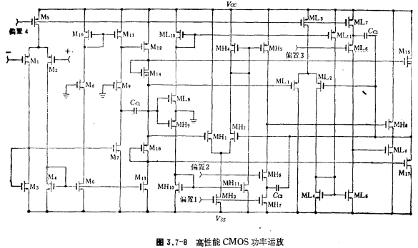
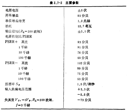
Figure 3.7-8 is a high-performance CMOS power operational amplifier, and its main parameters are listed in Table 3.7-3.
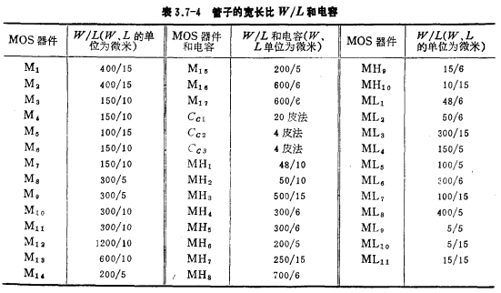
The preamplifier (M1~M11) in the figure has the same circuit structure as the high power supply rejection ratio op amp shown in Figure 3.6-4 in the previous section, so the power op amp shown in Figure 3.7-8 has a high power supply rejection ratio. The output stage in the figure is the same as the circuit in figure 3.7-6, MH1~MH11 constitute A1 amplifier, ML2~ML11 constitute A2 amplifier, MH3 and M15 provide positive output current, andM17, sink negative current, Cc1 Cc2 and Cc3 are the whisker rate compensation capacitors of the preamplifier, A1 amplifier and A2 amplifier, respectively. The W/L ratio of each tube in the figure is shown in Table 3.7-4.


Contact: Mr. Zou
Contact number: 0755-83888366-8022
Mobile phone: 18123972950
QQ: 2880195519
Contact Address: 5C1, Block CD, Tianji Building, Tianan Digital City, Chegongmiao, Futian District, Shenzhen
Please search WeChat official account: "KIA Semiconductor" or scan the following picture to "Follow" official WeChat official account
Please "follow" the official WeChat account: provide MOS tube technical assistance


