Electronic Technology Forum
Detailed CMOS power operational amplifier output stage circuit working principle diagram
1. Principle of CMOS output circuit
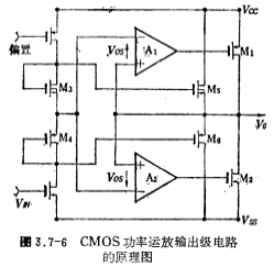
Figure 3.7-6 is a schematic diagram of the CMOS power operational amplifier output stage circuit. Its working principle is basically the same as that of the circuit in Figure 3.7-1 and Figure 3.7-2, but its performance is better than that of the circuit in Figure 3.7-2.

In the figure, the amplifier A1 and the output tube M1 constitute a full negative feedback amplifier, and its positive output gain is 1. The amplifier A2 and output M2 constitute a full negative feedback amplifier, and its negative output gain is also 1. Under static conditions, both M1 and M2 are in the cut-off state. At this time, the output circuit is borne by M5 and M6, and the quiescent current is provided by the M2 and M4 bias circuits. In order to ensure that under static conditions, M1 and M2 are cut off, so when designing A1 and A2 amplifiers, the offset voltage Vos is artificially introduced (the width-to-length ratio of the input differential pair tubes of the A1 and A2 amplifiers is slightly different). CMOS output circuit. The offset voltage of the A1 amplifier makes the output of A1 at a high potential. The offset voltage of the schematic diagram of the A2 amplifier makes the A2 output at a low potential, so that under static conditions, both M1 and M2 are in an off state, thereby reducing static power consumption. When the negative end of the input terminals of the A1 and A2 amplifiers is a positive input signal, the output voltage of A1 becomes low and M1 is turned on. At this time, A1 and M1 form a negative feedback amplifier with a gain of 1, and the positive output current is mostly provided by M1 , M5 only provides a small part. At the same time, the output end of the A22 amplifier is still at a low potential, and the M2 tube continues to remain off. CMOS output circuit. When the negative end of the input terminals of the A1 and A2 amplifiers are negative input signals, A2 and M2 form a negative feedback amplifier with a gain of 1, and most of the suction current flows into M2, and only a small part flows into M6, while M1 is in the cut-off state. Therefore, from the negative end of the input terminals of A1 and A2, the output stage circuit is a class A and B push-pull amplifier, and the gain is 1.
2. The actual circuit of CMOS power op amp
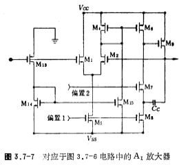
The actual circuit diagram of the A1 amplifier is shown in Figure 3.7-7.
In the figure, M1, M2, M4 and M55 constitute the input stage differential amplifier, M9 is the output stage circuit (ie the M1 tube in Figure 3.7-6), and Cc is the frequency compensation capacitor. When the positive input signal acts on the gate of the M1 tube, the current of the M2, M4 and M6 tubes decreases, and the gate potential of M9 drops, and the output current flows from M9 to the load. As the input signal increases, the M9 tube's current The output current also increases accordingly. CMOS output circuit. Under the action of the positive input signal, M13, M14 and M16 are in the cut-off state, which does not have any effect on the working state of the circuit, but the gate used for M1, that is, the gate of M13, is the negative input signal and is greater than At the threshold voltage of the M13 tube, the M13 tube is turned on, and its current flows through M14, so that M15 is also turned on. The current flows through M4, which increases the current of the M14 and M6 tubes, and the grid potential of the M9 tube rises. Deadline. CMOS output circuit. From the above discussion, we can see that the circuit in Figure 3.7-7 only amplifies the positive input voltage, and constitutes a negative feedback amplifier with a gain of 1, and its output current is provided by the M9 tube. When the negative input signal acts on the circuit, the M9 tube is cut off.

The circuit form of the A2 amplifier is the same as that of A2, as long as the n-channel MOS tube in the A1 amplifier is replaced with a P-channel MOS tube, and the P-channel MOS tube is replaced with an n-channel MOS tube, the actual circuit diagram of A2 can be seen in Figure 3.7-8 .
Contact: Mr. Zou
Contact number: 0755-83888366-8022
Mobile phone: 18123972950
QQ: 2880195519
Contact Address: 5C1, Block CD, Tianji Building, Tianan Digital City, Chegongmiao, Futian District, Shenzhen
Please search WeChat official account: "KIA Semiconductor" or scan the following picture to "Follow" official WeChat official account
Please "follow" the official WeChat account: provide MOS tube technical assistance


