Electronic Technology Forum
Schematic analysis and detailed explanation of CMOS power operational amplifier output stage circuit
Most of the CMOS operational amplifiers introduced above use a common source output stage circuit, so the output impedance is relatively high, and the driving force is relatively poor. CMOS power output stage circuit. This section will discuss CMOS power operational amplifiers with low output impedance, capable of driving large-capacity loads (including low-resistance loads) and low static power consumption. The design of CMOS power operational amplifiers includes two parts, namely preamplifier and output stage , And the design of the preamplifier is no different from the design of the various CMOS operational amplifiers discussed earlier, so this section mainly discusses the design method of the CMOS power operational amplifier output stage circuit.
1. Principle of CMOS output stage circuit
Figure 3.7-1 is the schematic diagram of the CMOS power operational amplifier output stage circuit. The A1 amplifier and the common source amplifier M1 constitute a full negative feedback amplifier; similarly, the A2 amplifier and the common source amplifier M2 also constitute a full negative feedback amplifier, that is, a voltage follower. Its voltage gain is and has a low output impedance. CMOS power output stage circuit. The main disadvantage of the circuit in Fig. 3.7-1 is that the quiescent operating current of the driving circuit M1 and M2 is difficult to determine due to the offset voltage of A1 and A2.
On the basis of the circuit in Figure 3.7-1, a practical CMOS power operational amplifier output stage circuit is given, and its schematic diagram is shown in Figure 3.7-2.
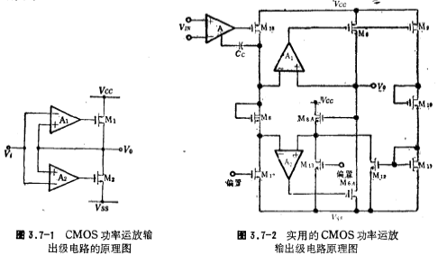
The amplifier A in the figure is used as the preamplifier of the output stage circuit, and Cc is the compensation capacitor of the preamplifier. The input signal is amplified by the input stage A amplifier and then added to For the gate, its source gets a larger amplitude signal. Positive half cycle signal through amplifier
 then sent to the output, because
 A negative feedback loop is formed. The signal amplitude at the negative input terminal of A1 is the same as the signal (output signal) at the positive input terminal of A1, which constitutes a negative feedback amplifier with a gain of 1. CMOS power output stage circuit. Negative half cycle signal through amplifier
 then sent to the output,
 form a negative feedback loop, the gain is also 1. Therefore, the output stage is a negative feedback amplifier with a gain of 1. Because of the deep negative feedback, the operating point is stable and has a low output impedance. When the drain signal voltage of M18 and M17 is in the positive half cycle, A1 drives M6 to provide current to the load.
 in a small current or cut-off state; when the drain signal voltage of M18 and M17 is in the negative half cycle, A2 drives
 , Draw current from the load, at this time
 in a small current or cut-off state, the output stage circuit shown in Figure 3.7-2 is a Class A and Class B push-pull amplifier.
In the picture , can make the output tube
 the quiescent current remains balanced and has a certain value. If the quiescent current of the M6 tube increases due to the offset voltage of the A1 amplifier, the M6 tube current increases, so
 the tube current also increases, passing
 as the current increases, its VGS voltage also increases. Since the output voltage is at a constant value (zero volts), a negative voltage is obtained at the positive input of amplifier A2, and the output voltage becomes negative to drive
 the gate voltage is reduced so that
 the current decreases.
From the figure and the above discussion, it can be seen that the offset of A1 and A2 can be determined by the source follower the amount of change of VGS to eliminate to ensure
 its operating current has a rated value under static conditions.
The negative feedback amplifier circuit A1 with a positive output gain of 1 is shown in Figure 3.7-3.
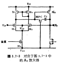
The differential amplifier is composed of M1~M5, and it and the common source amplifier It is composed of a negative feedback amplifier with a gain of 1. The Cc and MPC tubes in the figure constitute the frequency compensation of the amplifier. The circuit has a large positive common-mode input voltage range. CMOS power output stage circuit. When the input voltage is forward voltage,
 the increase of the VGS voltage of the tube increases the output current. In order to increase the output current as much as possible, in addition to increasing the transconductance of the M6 tube
 external should increase the maximum value of VGS
 .in
.in under conditions, M1 and M2 should still work in the saturation zone.
available from the picture

and

so

It can be seen from the formula (3.7-3) that increase , Should increaseM1, M2 tube threshold voltage
 in addition to the process guarantee for increasing the threshold voltage, the substrates of M1 and M2 are connected to the negative power supply Vss, that is, the substrate bias effect is used to make the threshold voltage
 . increase
 ,and
,and Increasing VT also increases accordingly, so as to ensure that with the input signal
 increase,
 the VGS of the tube, the voltage also increases, increasing the output current, and its maximum output current is determined by
 transconductance
 。
。
Regarding the structure of the negative output circuit A2, please refer to Figure 3.7-4. Its working principle is the same as that of the positive output circuit, so I will not repeat it here.
2. The actual circuit of CMOS power operational amplifier output stage
According to the schematic diagram in Figure 3.7-2, the output stage circuit diagram of the CMOS power operational amplifier is designed as shown in Figure 3.7-4. In the picture
 Constitute the A1 amplifier,
 Constitute an A2 amplifier,
 Is the output stage circuit of the op amp,
 these are the frequency compensation capacitors of A1 and A2. CMOS power output stage circuit. Now on the MOS tube in the picture
 To explain the function, when a large negative voltage is applied to the gate of the M1 tube, the drain-source voltage of the M5 tube is zero, and there is no current flowing through the differential amplifiers M1 and M2.
 Out of the tube, then
 the grid potential of the tube is floating, that is, uncertain, so
 the tube may not be in the cut-off state; when adding
 after the tube, make
 the gate potential of the tube is equal to the power supply voltage Vcc to ensure
 the tube is in a good cut-off state.
same the role of
 when the gate is a large forward voltage,
 the gate potential is Vss, so that
 the tube is in good cutting condition.
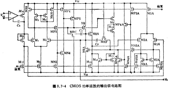
Figure 3.7-4 circuit also has current limiting performance, if over current, MP1 current increases, after
 ,make
,make the gate voltage rises, thereby reducing the flow through
 the current, which plays a current limiting role.
 the maximum current is limited to about 60 mA.
Finally, the frequency response of the circuit in Figure 3.7-4 will be explained. For the sake of simplicity, only the poles and zeros generated by the forward amplifier composed of A1 amplifier and M6 under open-loop conditions will be discussed. The AC equivalent circuit is shown in the figure. Shown in 3.7-5.
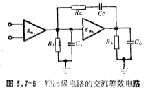
In the picture is the transconductance of the input differential amplifier,
 It is the transconductance of the
  tube. R1 and C1 are the output impedance and output capacitance of the input differential amplifier respectively. R1 and C1 are the load resistance and load diagram capacitance of the output terminal respectively. Rc and Cc are frequency compensation components. After calculation (refer to literature [16]), the zero and extreme rates are
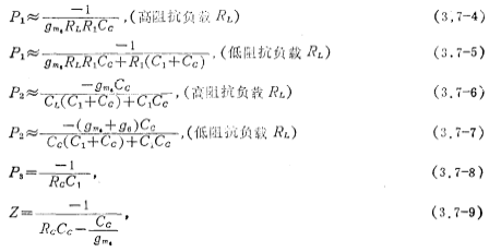
In the above formulas, P1 is the low-frequency pole (namely the main board point), P2 and P3 are the high-frequency poles, the output conductance of the tube, Z is the zero point. CMOS power output stage circuit. As long as the zero point is appropriately selected, the phase shift due to the pole can be eliminated, so that the circuit remains stable under closed-loop error conditions.
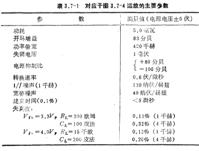
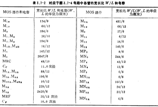
The main parameters of this circuit, device dimensions, and capacitance values are listed in Table 3.7-1 and Table 3.7-2, respectively.
Contact: Mr. Zou
Contact number: 0755-83888366-8022
Mobile phone: 18123972950
QQ: 2880195519
Contact Address: 5C1, Block CD, Tianji Building, Tianan Digital City, Chegongmiao, Futian District, Shenzhen
Please search WeChat official account: "KIA Semiconductor" or scan the following picture to "Follow" official WeChat official account
Please "follow" the official WeChat account: provide MOS tube technical assistance


