Electronic Technology Forum
Performance analysis of actual circuit of CMOS operational amplifier
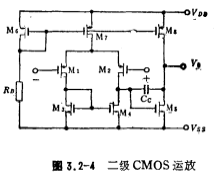
Figure 3.2-4 is a two-stage CMOS op amp whose input is a P-channel MOS pair tube. The CMOS four-op amplifier MC14573 produced by the American Motorola Company and the CMOS four-op amplifier 5G14573 produced by the Shanghai Component No. 5 Factory all adopt this circuit structure. Change the bias resistance the resistance value can adjust the operating current, gain, output current and other parameters of the op amp.

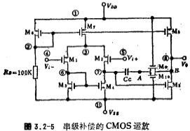
In order to improve the stability of the operational amplifier in Figure 3.2-4 and eliminate the zero point, a resistor R can be connected in series with the compensation capacitor image.png. Usually image.png. It can be replaced by a MOS tube, and its circuit form is shown in Figure 3.2-5.

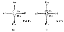
In the figure, the equivalent resistance between the drain and source of M9 and M10 is used to form the above-mentioned series electrical diagram. Here, the gates of the n-channel MOS tube M1 and the P-channel MOS tube M10 are connected to the positive and negative power supply voltages, respectively. When the polarity of the output signal is different, their drain and source functions are interchanged. In the static state, there is no current in M9 and M10. When the signal is input, if the output signal of the circuit is positive, the potential at point B is higher than the potential at point A. At this time, M9 is in a positive working state, and M10 is in a reverse working state (its source and drain are interchanged), as shown in Figure 3.2-6a. On the contrary, when the output signal of the circuit is negative, The potential at point B is lower than the potential at point A, then M9 is in the reverse working state, and M10 is in the forward working state, as shown in Figure 3.2-6b. Generally, in integrated circuits, the forward and reverse characteristics of MOS transistors are identical. According to the AC small signal equivalent circuit, the equivalent resistance between the two ends of A and B can be obtained ,Here gm is the transconductance of M9 and M10. Therefore, when the transconductance of M9 and M10 is designed to be
 when the transconductance is similar, the circuit can eliminate the capacitance
 caused zero point.

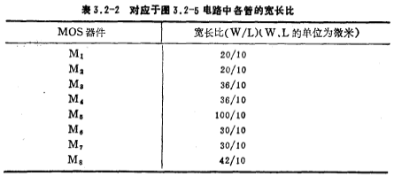
Now the ratio of width to length of each tube in the circuit of Figure 3.2-5 is listed in Table 3.2-2.

Contact: Mr. Zou
Contact number: 0755-83888366-8022
Mobile phone: 18123972950
QQ: 2880195519
Contact Address: 5C1, Block CD, Tianji Building, Tianan Digital City, Chegongmiao, Futian District, Shenzhen
Please search WeChat official account: "KIA Semiconductor" or scan the following picture to "Follow" official WeChat official account
Please "follow" the official WeChat account: provide MOS tube technical assistance


