Electronic Technology Forum
The working principle and parameter explanation and analysis of CMOS operational amplifier
After the circuit structure of the CMOS operational amplifier is determined, the most important thing is to determine the operating current and operating voltage of the operational amplifier at all levels. In order to make the op amp work normally, first of all, it is necessary to ensure that the FETs in the amplifiers of all levels of the op amp are in the saturation zone under static and specified dynamic conditions; secondly, under static conditions, when the input terminal is equal to zero voltage, the output terminal voltage is Zero means that there should be a small offset voltage; thirdly, determine the operating currents of the amplifiers and bias circuits at all levels according to the gain and output dynamic amplitude. We know that the working current and voltage of the MOS tube are determined by the process parameters and the width-to-length ratio of the channel. If the working voltage (VG1) is also determined after the process parameters are determined, the working current ID of the MOS tube is only related to the width-to-length ratio of the channel. Therefore, in the MOS operational amplifier, the operating points of the amplifiers at all levels are closely related to the channel width-to-length ratio of the MOS tube. Below we take the commonly used CMOS operational amplifier circuit as an example to analyze, in order to make the MOS operational amplifier have a small offset voltage, how to determine the channel width-to-length ratio of the MOS tubes in the amplifiers at all levels.
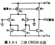
Use the circuit shown in Figure 3.2-1 to analyze the input offset voltage.

Here, the factors that affect the input offset voltage of the circuit include the input offset voltage of M1 and M2 itself and the influence of the mismatch of M3 and M4 tubes (denoted as ), And the influence of the later stage (denoted as
 ), So the total input offset voltage of the circuit
 for
for

According to the discussion in Section 5 of Chapter 2, for
for

1. Offset voltage
It must be pointed out that the offset voltage of the above formula the expression of is obtained under the symmetrical conditions of the input pair tube M1, M2 and the current source tube M3, M4. It is determined by the process parameters (such as uneven diffusion, uneven oxide layer thickness), plate making, photolithography, etc. The random offset voltage introduced. To reduce this random offset voltage, the process conditions should be improved, plate making, and lithography accuracy should be improved. In addition, when designing the layout, the input pair M1, M2 and the current source pair M3, M4 should be as close as possible to reduce Threshold voltage difference of M1 and M2 tube
 and M3、M4 the difference of the threshold voltage of the tube
 , And appropriately increase the size of the tube to reduce the relative error of the channel width and length of M1, M2 and M3, M4.
second section The imbalance is mainly caused by the second stage. Because the MOS transconductance is small, the differential gain of the input stage is not very large, so the offset caused by the second stage is referred to the offset voltage of the input terminal
 can't be ignored.
If the input pair tube M1, M2 and the current source pair tube M3, M4 are symmetrical, when the input voltage is zero, the drain-source voltage of the M3 tube is equal to the drain-source voltage of the M4 tube, as shown in Figure 3.2-1

Since the process parameters and threshold voltages of the M3, M4 and M5 tubes are the same, according to the current expression of the MOS tube and the formula (3.2-2), we can get

Obviously to make the offset voltage zero, the current Io of the M5 tube should be the same as the current IT of the M7 tube, and the M7 tube and the current source tube M5 of the input stage differential amplifier have the same bias voltage, so Io (the working current of the M5 tube) ) It has the following relationship with IT:

because , Then by (3.2-4) and (3.2-5) formulas can be obtained

because , The above formula can also be written as

Therefore, if the ratio of the channel width to length ratio of (M3+M4) to M6 is equal to the ratio of the channel width to length ratio of M5 and M7, the latter stage has no effect on the input offset voltage. If these ratios are mismatched or the threshold voltage of the relevant tube is mismatched, it will cause an increase in the input offset voltage. However, if the gain of the differential amplifier of the input stage is large, the offset caused by the mismatch of the subsequent stage can be reduced. After the channel width to length ratio of the MOS tube of the amplifier is determined, the operating current is determined according to the requirements of voltage gain and output dynamic range. The working current is provided by the bias circuit. The following discusses how to determine the operating point of the CMOS operational amplifier, and introduces the parameter selection of the MOS tube (mainly the channel width-to-length ratio).
2. Working point and pipe parameters
Figure 3.2-2 is a typical two-level CMOS op amp. RB and M6 constitute a bias circuit to provide the working current of the input stage differential amplifier and the output stage circuit. The differential amplifier is composed of differential pair tubes M1, M2, active loads M3, M4, and M7 as a current source tube. M5 and M6 constitute the second stage common source amplifier. capacitance it is the frequency compensation capacitor.
After the operational amplifier structure is determined, first determine the DC operating point.
Now set VDD=5V, Vss=-5V, and the threshold voltage of the tube▕VT▏=1V. Considering the dynamic amplitude of the output, set the potential of node ② in the figure to -2 volts, that is volt. Considering the power consumption of the circuit, the gain of the amplifier, the driving ability of the output, etc., select the bias current
 microampere, the working current of the differential amplifier
 microampere, output stage circuit
 microampere. According to the operating current, the bias current resistance RB is

Suppose the  parameter of the NMOS tube is

Then the aspect ratio of M6 is

Similar to the formula (3.2-6), the aspect ratio of  is calculated by the following formula

Under static conditions (input voltage is zero), in order to make the offset voltage zero, you should use , According to Figure 3.2-2 and relational formula (3.2-6), we can get
 the tube width to length ratio is

The gain of the differential amplifier in the figure can be written as

In the formula, λ is the channel length modulation parameter.
Assume Vol-1, while
 microampere,
 microampere/volt2, then (3.2-9) is expressed as

The second stage gain is

where microampere/volt2,
 microampere, λ=0.01 Volt-1. Therefore, the above formula can be written as

To make the transconductance gm of the second stage greater than the transconductance of the input stage differential amplifier ,choose

From the formula (3.2-8), the width-to-length ratio of M3 and M4 tubes is

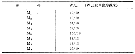
Now the width-to-length ratio of each tube in the circuit in Figure 3.2-2 is listed in Table 3.2-1

At this time, the voltage gain of the op amp shown in Figure 3.2-1 is

The output impedance of the op amp is

The transconductance of the first stage of the op amp is

The transconductance of the second stage of the op amp is

If the unity gain bandwidth GB of the design op amp is 1 MHz, then according to the formula (3.1-3) in the first section, the compensation capacitor Value is

The zero point of the op amp is

The first pole of the op amp:

The second pole of the op amp is related to the load capacitance CL, and its value is

According to the discussion in the first section and the formula (3.1-7), the load capacitance CL should be less than 23 picofarads, otherwise, high frequency oscillation may occur when the operation is in deep negative feedback. CMOS operational amplifier. In order to improve the stability of the operational amplifier and eliminate the zero point, the method is to use frequency compensation capacitors with resistance
 Compensation after series connection, and
 . The circuit form is shown in Figure 3.2-3.
relevant information
The actual circuit of CMOS op amp
Contact: Mr. Zou
Contact number: 0755-83888366-8022
Mobile phone: 18123972950
QQ: 2880195519
Contact Address: 5C1, Block CD, Tianji Building, Tianan Digital City, Chegongmiao, Futian District, Shenzhen
Please search WeChat official account: "KIA Semiconductor" or scan the following picture to "Follow" official WeChat official account
Please "follow" the official WeChat account: provide MOS tube technical assistance


