Electronic Technology Forum
MOS operational amplifier frequency compensation/resistance capacitor amplifier for analysis
The above discussion shows that when performing phase compensation in a MOS operational amplifier, the negative effects of the zero point in the circuit must be eliminated. In order to better explain the frequency compensation of the MOS operational amplifier, we will discuss the formula (3.1-2).
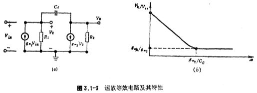
If the frequency of the high frequency pole P2 and the zero point Z of the MOS operational amplifier is greater than the unity gain bandwidth GB. At this time, when the voltage gain of the op amp is higher than the frequency of the low-frequency pole P1, it drops by -20dB/10 octave (see Figure 3.1-1), and the unity gain bandwidth should be

C1 in the equivalent circuit is the internal distributed capacitance, which is the same as the compensation capacitance compared with the load capacitance CL, it is very small, so P2 can be approximated as

From (3.1-3), (3.1-4) and zero point expression (3.1-2), we can get

From equations (3.1-5) and (3.1-6), it can be seen that the ratio of the zero point Z of the right half plane, the high-frequency pole P2 and the unity gain bandwidth GB is determined by the ratio of gm1/gm2, so that the MOS operational amplifier needs to achieve a single-pole response. , That is, there is only one main pole P1 above 0 decibels, and the high pole P2 "GB, zero Z "GB, then the ratio of gm1/gm2 should have the following relationship:

Obviously, the greater the ratio of gm1/gm2, the better the stability of the MOS operational amplifier. And compensate the e-passenger the value of is related to the size of the load capacitor CL, C1 increases,
 also increase accordingly.
From the previous discussion, it can be seen that the transconductance gm of the second stage amplifier of the MOS op amp is much larger than the transconductance gm of the first stage amplifier. It is quite difficult. In addition to the design considerations of the MOS op amp, there is another point that is the MOS tube. The transconductance is only proportional to the square root of the operating current.
To improve the stability of the MOS operational amplifier, in addition to the design of a large gm1/gm2 ratio, the elimination of the zero point (Z) can be used to improve the stability of the circuit. There are two ways to eliminate the zero point:
1、Isolate the compensation capacitor  from the output of the amplifier
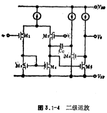
In this scheme, the output of the second stage is connected to the compensation capacitor through a follower. The circuit structure is shown in Figure 3.1-4. At high frequencies, due to source follower isolation, capacitance
  it is not possible to feed the signal directly to the output of the amplifier. Thereby reducing the phase change of the output signal of the operational amplifier. The compensation schematic diagram and equivalent circuit of this figure are shown in Figure 3.1-5a and Figure 3.1-5b respectively.
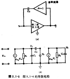
From Figure 3.1-5b, the nodal equation is

To solve the above equation, the transfer function is

It can be seen that the compensation capacitor after the isolation amplifier, the zero point is eliminated, because
 , The low-frequency pole P1 and the high-frequency pole P2 of the above formula are simplified to

Compared with formula (3.1-11) and formula (3.1-2), the poles P1 and P2 do not change much, but the zero point is eliminated, and the stability of the circuit is improved.
2、The compensation capacitor  is connected in series with the resistor to be compensated
Another effective way to eliminate the zero point of the right half plane is the capacitor with resistance
 Compensation is performed after series connection, and the equivalent circuit is shown in Figure 3.1-6.
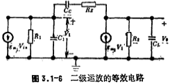
From the graph, the following nodal equation
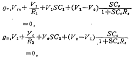
Solving the above equation, the transfer function is obtained as

where

if , The two poles are far apart, then the poles and zeros obtained from equation (3.1-12) are

From the formulas (3.1-12) and (3.1-13), when , The zero point is eliminated, which improves the stability of the circuit. If R1 is slightly larger than 1/gm, the zero point is moved from the right half plane of the S plane to the left half plane, which can also improve the stability of the circuit.
Contact: Mr. Zou
Contact number: 0755-83888366-8022
Mobile phone: 18123972950
QQ: 2880195519
Contact Address: 5C1, Block CD, Tianji Building, Tianan Digital City, Chegongmiao, Futian District, Shenzhen
Please search WeChat official account: "KIA Semiconductor" or scan the following picture to "Follow" official WeChat official account
Please "follow" the official WeChat account: provide MOS tube technical assistance


