Electronic Technology Forum
MOS Operational Amplifier Classification Principle Features and Application
MOS operational amplifier is abbreviated as operational amplifier, which is divided into two categories: NMOS operational amplifier and CMOS operational amplifier: The so-called NMOS operational amplifier is the field effect tube in the operational amplifier is composed of NMOS transistors; CMOS operational amplifier is the field effect tube in the operational amplifier It is composed of P-channel and N-channel MOS transistors.
The design of MOS operational amplifier is similar to that of bipolar operational amplifier. It is mainly considered from the aspects of open loop gain, output swing, common mode rejection ratio, frequency characteristics, transient response, offset voltage and power consumption, but MOS operational amplifier has its own The characteristics of are different from bipolar op amps in some respects, and are explained as follows:
(1) MOS operational amplifier and bipolar operational amplifier
Compared with bipolar operational amplifiers, MOS operational amplifiers have the biggest advantages of high input impedance (above 1010 ohms), small input biasing plate (10-13~10-12 amperes), low power consumption and large voltage gain. Therefore, in recent years, MOS operational amplifiers, especially CMOS operational amplifiers, have been rapidly developed and become an indispensable basic component in large-scale analog integrated circuits.
(2) Bipolar operational amplifier
It usually appears in the form of a monolithic integrated circuit and has good electrical performance and versatility. The MOS operational amplifier is usually used as a basic unit in integrated circuits, such as switched capacitor networks, A/D, D/A and other MOS integrated circuits. Therefore, when designing MOS operational amplifiers, the versatility of MOS operational amplifiers is not emphasized, but According to the overall performance of the integrated circuit, the basic parameters of the MOS operational amplifier are determined, such as the open-loop gain and drive capability of the MOS operational amplifier. As a basic unit in the MOS integrated circuit, the MOS operational amplifier is loaded by the high impedance of the MOS tube. Devices and capacitors, so the design of MOS op amps usually does not require low output impedance, but should have the ability to drive capacitive loads. In addition, as the scale of MOS circuits expands, digital circuits and analog circuits are integrated (such as A/D, PCM codec, etc.). At this time, it is necessary to consider the effect of switching noise of the digital circuit on the analog circuit of the MOS operational amplifier through the power supply. , This requires MOS operational amplifiers to have a higher power supply voltage rejection ratio (PSRR). The smaller the change in the output voltage of the op amp caused by the change in the power supply voltage, the stronger the power supply voltage rejection ratio capability.
(3) MOS equivalent bipolar device
Compared with bipolar devices, MOS has greater noise, especially 1/f noise at the low-frequency end. Therefore, when designing MOS operational amplifiers, you should consider how to reduce the noise of the operational amplifier. The noise mainly comes from the input stage, and the op amp input is made up of a differential amplifier. Therefore, reducing the noise of the input differential amplifier can reduce the op amp noise.
(4) Threshold voltage of MOS tube
The threshold voltage of the MOS tube is relatively large, so there is a large offset voltage. When designing and manufacturing MOS operational amplifiers, the threshold voltage of the MOS tube should be reduced, and efforts should be made from the layout design and process to obtain a low offset voltage. .
(5) MOS tube transconductance gm
The transconductance gm of the MOS tube is low, and the transconductance is proportional to the square root of the working current ID, which makes the frequency compensation of the MOS operational amplifier more complicated than the bipolar type (discussed in detail below).
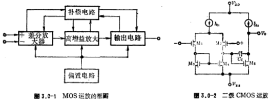
The diagram of the MOS operational amplifier is shown in Figure 3.0-1. The high-gain stage in the figure is usually a common source amplifier circuit. The compensation circuit is usually a frequency compensation capacitor, which is connected between the input and output of the high gain stage to realize the frequency compensation of the operational amplifier.
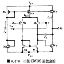
The common circuit form of CMOS operational amplifier is shown in Figure 3.0-2. It consists of a two-stage amplifier, the first stage is a differential amplifier circuit composed of M1~M4, and the second stage is A common source amplifier composed of current source Io2, this two-stage amplifier provides a gain of about 1000 to 20000 times. The capacitor Co is a frequency compensation capacitor. The actual circuit is shown in Figure 3.0-3.

In the picture and
and form a bias circuit to provide a reference current IR,
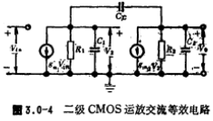
 it forms a current source circuit with the bias circuit to provide the working current of the differential amplifier and as the active load of the M5 common source amplifier. Its equivalent circuit of AC small multiple is shown in Figure 3.0-4.

Among them, R1 and C1 are the equivalent resistance and distributed capacitance at the input of the second gain stage, respectively, and R1 is the output impedance of the differential output terminals M2 and M4. in parallel, namely
 Are the resistance and capacitance at the output of the second gain stage, R2 is the output impedance of the output amplifiers M5 and M6
 In parallel, namely
 , The capacitance CL is mainly the load capacitance of the output terminal.
 They are the equivalent transconductances of the first stage and the second stage of the amplifier. Obviously, the DC voltage gain of the circuit is

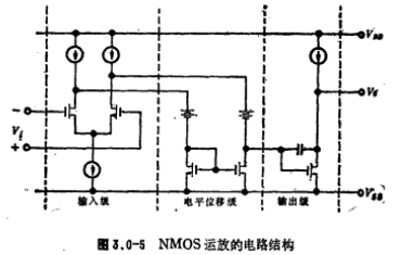
Figure 3.0-5 shows the circuit structure of a general NMOS operational amplifier, which is usually composed of three parts: an input differential amplifier, a level shift circuit, and an output stage common source amplifier. Since NMOS operational amplifiers are all composed of NMOS transistors, the level configuration between stages is difficult, and the circuit structure is complicated. In order to obtain higher gains, three or more amplifiers are required. This brings difficulties to frequency compensation. Therefore, NMOS Compared with CMOS operational amplifiers, operational amplifiers have obvious shortcomings. However, since the speed and integration of NMOS circuits are higher than those of CMOS circuits, NMOS operational amplifiers are sometimes used in large-scale MOS analog integrated circuits. In fact, the first full MOS operational amplifier circuit is an NMOS operational amplifier.

Relevant information
Nodal equation of equivalent circuit
Op amp equivalent circuit and its characteristics
Frequency compensation of MOS operational amplifier
Contact: Mr. Zou
Contact number: 0755-83888366-8022
Mobile phone: 18123972950
QQ: 2880195519
Contact Address: Block 5C, CD Block, Tianji Building, Tianan Digital City, Chegongmiao, Futian District, Shenzhen
Please search WeChat official account: "KIA Semiconductor" or scan the following picture to "Follow" official WeChat official account
Please "follow" the official WeChat account: provide MOS tube technical assistance


