Electronic Technology Forum
Detailed explanation of the bias circuit based on the transistor VBE voltage
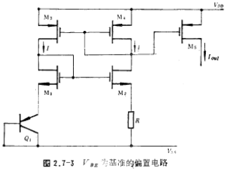
The bias circuit based on VBE is shown in Figure 2.7-3, where the PnP transistor Q1 and the CMOS tube are formed at the same time.
The feedback loop formed by M1~M4 forces the current flowing through the Q1 tube to be the same as the current flowing through the resistor R. From the figure, the following relationship can be obtained

scilicet

This formula shows that the bias circuit in Figure 2.7-3 also has a large negative temperature coefficient.

Contact: Mr. Zou
Contact number: 0755-83888366-8022
Mobile phone: 18123972950
QQ: 2880195519
Contact Address: 5C1, Block CD, Tianji Building, Tianan Digital City, Chegongmiao, Futian District, Shenzhen
Please search WeChat official account: "KIA Semiconductor" or scan the following picture to "Follow" official WeChat official account
Please "follow" the official WeChat account: provide MOS tube technical assistance


