Electronic Technology Forum
MOS memory-random access memory (RAM) structure and characteristics of the reading and writing process
In MOS integrated circuits, it can be divided into small-scale integrated circuits according to the complexity of the circuit and the number of components contained in each chip. , Medium-scale integrated circuits
 Large scale integrated circuit
 And VLSI
 . It is generally believed that each chip contains less than 100 components, which is a small-scale integrated circuit; 100 to 1,000 components are medium-scale integrated circuits; those with more than 1,000 components are large-scale integrated circuits; and 100,000 components or more are very large-scale integrated circuits. MOS random access memory ram.
In the field of MOS large-scale integrated circuits, the most important position is memory, such as serial memory composed of shift registers, random access memory (RAM), read-only memory (ROM) And several types such as programmable read-only memory. The charge-coupled device (CCD), which is similar to the basic structure of the MOS device, has the advantages of simple structure and wide range of use, and has developed extremely rapidly at present, and has become a rookie of large-scale integrated circuits.
This chapter mainly introduces the working principle and circuit structure of random access memory, read-only memory and charge coupled device in MOS memory.
MOS memory
MOS memory is a functional component that can access logical information. A large amount of memory can form a storage system. It is one of the main components of various types of electronic computers and is widely used by other electronic technologies. use. MOS random access memory ram, like the human cerebral cortex, can store the instructions and calculation data needed for computer work, or take it out as needed. The demand for memory is huge, and its performance directly affects the level of electronic computers.
1. Random Access Memory (RAM)
Random access memory (RAM) is composed of many storage units, and each of its storage units can store or take out the required binary information in a certain required order. There are two types of MOS random access memory, static and dynamic. Dynamic RAM has the advantages of low power consumption, high integration, and fast speed; static RAM has stable performance and is easy to use.
A complete MOS memory system should include memory array, address register, address decoder, read/write driver, regeneration amplifier, read/write control, data register, timing pulse generator and other components, as shown in Figure 4- 1 shown.
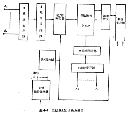
Below we will focus on the structure of the storage unit in the memory and its storage principle, and briefly introduce the complete structure of several typical memories in conjunction with the working principle, so as to have a complete understanding of the random access memory.
1. Static MOS storage unit
(1)Single channel six-tube static storage unit
Figure 4-2 shows the six-tube static storage unit, which is the smallest repeating unit in the static MOS RAM array, which can store two types of information 1os, "1" or "0". The static MOS memory cell is essentially a flip-flop, which is composed of two mutual feedback inverters. In order to be able to read or write data, the MOS random access memory ram connects two coupling devices controlled by the read/write bit line D to the two output terminals of the basic flip-flop. , As the gate control tube, the gates of the two gate control tubes are connected to the word line. The flip-flop is coupled to the bit line through the gate control tube. In the process of reading and writing, an addressing pulse must be added on the word line first to make a certain unit selected. The following describes its read/write process.
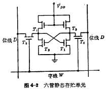
①Write When this unit is selected (that is, a "1" pulse is added to the word line W), make Conduction. If you want to write "1" into the cell, you need to add a "1" level to the D line.
 add "0" level on the line to make
 due,
due, on, that is, "1" is written into the cell. If you want to write "0", just add a "0" level to the D line,
 add "1" level to the line to make
 Conduction,
 At this time, "0" is written into the cell.
When the unit is written with "1" or "0", the word selection pulse passes to make turn off, the "1" or "0" written into the basic trigger will stabilize for a long time.
②read out When the information stored in the unit is to be read, first make this unit selected, so that Conduction. If "1" is stored in the cell, then
 Conduction,
 Cut off, bit line
 经
经 grounded. because
 It is directly connected to the sense amplifier, so that the ground potential is connected to the sense amplifier and read out in the form of voltage. Of course, MOS random access memory ram can also be read and output in the form of current, because
 Connecting to the ground, there is a current through the sense amplifier to the ground, this current is sensed by the sense amplifier and discerned, it means that the unit contains "1" information. if
 If there is no conduction, no current will flow, which means that "0" is stored in the cell.
(2)CMOS six-tube static storage unit
Utilize two OMOS inverters to couple with each other, and add appropriate coupling device, form the static memory cell of CMOS structure, as shown in Fig. 4-3. in for two coupling gates.
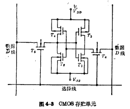
Since the turn-on voltage of the N-channel device is relatively low, and the mobility of the carrier is large, the coupling device N-channel MOS tubes are mostly used.
CMOS structure is used to compose the storage unit, which has some uniqueadvantage:
①Low power consumption The static power consumption per bit is about 10nW, and only a limited amount of power consumption is consumed during the dynamic process of conversion.
②Adopt a single working power supply The power supply voltage has a large variation range, and it can work between 3~16V.
③Strong anti-interference performance Up to 50% 。
。
The disadvantage is that the degree of integration is lower than that of a single-channel MOS memory cell.
2、Dynamic MOS memory cell
The static storage unit has a large number of tubes and the unit occupies a large area, which is not conducive to the development of large-capacity storage. In order to reduce the unit area and improve integration, dynamic four-tube, three-tube and single-tube units have been developed. The structure and working principle of these dynamic memories are respectively introduced below.
(1)Four-tube dynamic memory
Dynamic memory relies on the temporary storage effect of the charge on the node capacitance to store information. Its work is carried out under the control of clock pulses. Since the time for storing electric charge in the capacitor cannot be too long, it is required to refresh the stored information regularly.
①Storage unit
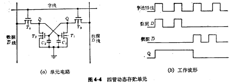
Figure 4-4 (a) Four tubes form a four-tube dynamic storage unit, of which
 is the storage tube,
 The tube is a gated tube, and in terms of form, the six-tube unit saves two load tubes. When the unit is not selected,
 and
and at the end, the storage unit is in the maintenance state, and the information exists
 gate node capacitance
 superior.
②Principles of Reading and Writing
The reading and writing of the storage unit is divided into three parts: writing "1", writing "0" and reading.
a.Write“1”When the word select line is "1" level, make Turn on, and add "1" level to the data line D respectively, in
 Add "0" level on the line, so
 Is charged so that
 Conduction while
 through
 Discharge to ground to make
 Deadline. In this way, "1" is stored in the unit (ie
 )。
)。
b.WriteThe "0" situation is similar to writing "1". When the word selection pulse comes, as long as the Add "1" to the line, and add "0" to the D line. At this moment
 be charged,
 turn on
 Pass
Pass Discharge to ground to make
 deadline. Then "0" is written into the cell.
0.read out In the read operation, first make the data line D and Both are 1. When the unit is selected, if the original "1" stored in the storage unit, because
 Conduction, there will be current from
 thread warp
 To ground, this current can be detected by a sense amplifier. MOS random access memory ram. and
 Is cut off,
 There is no current flowing in the circuit of line D and data, so line D still maintains the "1" level, and at the same time through
 对
对 charge to refresh the signal and restore the original leaked charge.
If the original stored signal is "0", the result is opposite to the above, and finally D=0, ,As shown in Figure 4-4(b).
From the analysis of the dynamic four-tube unit, it can be seen that during the read operation, there is also a refresh process.
③Memory map
In order to let everyone have a complete concept of the work of random access memory, the complete structure and working principle of 1024-bit dynamic RAM are introduced below. The 1024-bit RAM shown in Figure 4-5 is made of silicon sugar N-channel technology, and the storage array is composed of four-tube dynamic cells. Its composition is as follows:
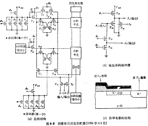
a. Storage matrix consists of 32 rows×32 columns of storage units, with a capacity of 1024 words×1 bit. The word selection lines of all cells in the same row of the storage matrix are connected together, a total of 32  Select line, respectively connect to
  of the decoder The output terminal. The data lines of all units in the same column are connected together through the gate on the column data line (ie bit line)
  ,..., etc. are connected to the data bus, and the gate on the data line is controlled by
  Select line control, when a certain
  When the selection line is at "1" level, the data line is connected to the data bus.
b. Pre-charge tube There are pre-charge tubes on each data line, such as  Tube. The power supply voltage of the pre-charging tube is
  . The grid of the precharge tube is controlled by the clock pulse
  . When
  ,
,  Turn on, so that all data lines are charged to
  .
.
C. Address decoding buffer There are ten address buffers,  direction and
  There are five in each direction, as shown in Figure 4-5(b).
The output ends of the address decoding buffer are respectively connected with the input ends of the decoder,  The input terminal of the decoder is
  and
and  ,
, The input of the decoder is
  and
and  . The normal operation of the buffer requires two-phase clock pulse
 and
and  Control. When
  ,
,  and
and  Turn on to make the output
  and
and  are both "0". MOS random access memory ram. Since the output of the address buffer is connected to the input of the address decoder, all address inputs are "0". When
 After that,
 The pulse comes, so
 Connected, so according to
 input, the address decoding buffer will have the corresponding
 and
and output, the address decoder also There is a corresponding input.
d. Read and write circuit Each column data line is connected to the data bus through the strobe gate of the column line, and the data bus is controlled by the chip select The gatekeeper  is connected with off-chip data (in/out) lines . When
  is turned on, the selected unit can be read and written. If
  , the data input and output lines and the data of the entire memory The bus is disconnected and cannot be read or written.
e.Decoder and driver Each output line of the decoder has to control 64 transmission tubes of 32 storage units. The capacitance is very large, so a driver is needed. Driver by MOS tube and capacitance
 composition,
 Connected at
 Between the gate and drain of the tube, it is called a bootstrap capacitor, and its structure is shown in Figure 4-5(c). This is a dual value capacitor. when
 When the inversion layer channel is connected to the drain, the capacitance is very large;
 at this time, only the cover capacitance between the gate and the drain is close to zero. The drain of the drive tube is connected to the address strobe pulse
 when
when time, the one strobed
 Although turned on, the "word" selection line of the memory matrix is still at the "0" level, so the cell is still not strobed. Only if
 At this time, the "word" selection line of the selected row is high. Due to the existence of bootstrap capacitor, when
 When rising from "0" to "1", the gate potential of the drive tube also rises at the same time, so that
 The on-resistance becomes very small, so the driving ability is very large, which can make the word selection line quickly charge, and the bit line transmission tube will quickly turn on, so it is beneficial to increase the speed.
The entire RAM requires three sets of power supply voltages;  , substrate reverse bias voltage
 . There are also three-phase clock pulses
  and
and  are chip select pulses, their high level is 12V, and the low level is less than 0.5V.
Let’s introduce its read, write and refresh operations;
a.write write start, clock pulse 
 , the chip select pulse
  Keep all of them
"0". Under the action of  , the output of the address buffer
  are all "0", the input of the decoder is low, and the output is both It is high level. On the other hand, the 32-column data cables are all charged to a high level.
 . When the
  pulse ends, due to the small leakage current, the bit line The potential remains unchanged.
When From "1" to "0",
  began to arrive. At this time, according to the input of the address buffer, the output of each address buffer is determined. The output of the address buffer is connected to the input of the address decoder, resulting in
  Address decoder and
  Address decoder One of the output lines is selected. For example, if the address code is 0000000000, there are only 32
  decoders The first output is high, and all others are low. At the same time 32
  only the first bit line is used in the decoder The gate control tube is turned on, and the others are turned off.
When After that, follow
  and chip selection signal
  is here, let the door control
 is on. The data to be written is sent to the input/output line. If you want to write "1", add the "1" level to the input/output line D, in
  Add "0" level to the line. Since
  is connected, the data will be connected to the selected one through the data bus A series of data lines are connected to write the selected cells in the first row and first column.
b. Read out When reading out, make the input terminal  and
and  are all high levels. When
  and
and  is "1", after the selected unit is connected to the data line, it is connected to the conducting tube in the unit There is current flowing through the data line. For example, when
  is turned on, there will be current passing through the D line;
  is turned on, then there is a current passing through the universal line, and this current passes After the sense amplifier outside the bus is amplified, it can be judged whether the unit is "0" or "1".
c. Refresh As everyone knows, the memory has a "refresh" function during the reading process. When reading, other memory cells that are not selected on the same word line, their bit lines are not connected to the data bus, so the bit line pre-charge tube (such as  ) The cell should be "refreshed" through the gated transistor that is turned on to supplement the charge leaked from the gate capacitor. The memory also has a special "refresh" operation, which is performed line by line at regular intervals. Its method is the same as the read operation, but don't add chip select signal. MOS random access memory ram. The refresh process is carried out line by line. In one refresh cycle, 32 rows need to be refreshed. The time required to refresh a row is roughly equal to the read cycle time. In order not to lose the stored content, it must be refreshed periodically, for example, every 2ms, and reading and writing cannot be performed during the refresh time.
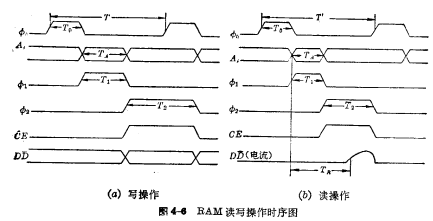
Figure 4-6 (a) and (b) are the working timing diagrams of memory writing and reading respectively. Where  is the pre-charge clock pulse width, which must be ensured in the data line Establish a stable 5V level on
 . This depends on the on-resistance of
  in Figure 4-5 And the distributed capacitance of the data line.
  is the pulse width of the address code, it must be ensured that it is not selected The output terminal of the decoder is discharged to zero at high level. This depends on the equivalent time constant of the decoder input tube
  .
. 是时钟。和片选信号
 The pulse width, which is to make the selected word line gate control
  And the chip selection tube
  After being fully connected, the input data is in the data The time to establish a stable level on the line and make the memory cell become the stable state required for writing. If it is a read, the time for the read data current to stably appear at the output end is guaranteed. The former depends on the on-resistance of the
  tube, the distributed capacitance of the data line and The flip time of the memory cell flip-flop; the latter depends on the on-resistance of these tubes.
The time parameters that indicate memory speed are: access time (fetch time) and cycle time. The access time refers to the time from the input of the address code to the output of the valid data. It includes the delay of the address decoder and the delay on the readout circuit after the chip select signal is added. . The cycle time refers to the basic time period for the memory to complete a certain operation, so it is also called the cycle period. The so-called certain operations refer to various operations during read-write or write-read. The cycle period refers to the longest of the above-mentioned various operations.
  in Figure 4-6 indicates that the writing is completed before proceeding The cycle of the next operation, and
  means that it will be read after reading The cycle for the next operation. The cycle period is determined by the larger of the two.
(2) Three-tube dynamic memory
①Three-tube storage unit
The memory of the three-pipe unit is currently the most widely used memory. There are three different forms of storage units:
a. unit This is the most basic three-pipe unit circuit, as shown in Figure 4-7(a), which consists of
  three It consists of a tube, two read-write select lines, two read-write data lines, and a ground wire. Where
 is the storage tube;
  is the readout control tube,
 is the writing control tube. The information is stored in
 the gate node of the tube On the capacitor, if
 Storage signal 1 at both ends ", then
 on, if
 the information stored at both ends is "0", then
 to.
to.
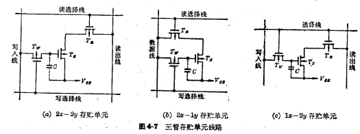
b. Unit This is composed of three MOS tubes, two read-write selection lines and a data line, as shown in Figure 4-7(b) as shown. Where
 The role and above< img src="http://www.kiamos.cn/userfiles/images/2020/11/16/2020111614541994.png" title="image.png" alt="image.png" style="font-size: 18px ; text-indent: 32px; white-space: normal;"/>the same unit. Since the two data lines are combined into one, the area can be reduced and the integration level can be improved. However, since only one wire is used for writing and reading data, it is necessary to add a read and write control circuit.
c. Unit Figure 4-7(c) is the circuit of this unit. As you can see from the figure, the read and write selection lines are combined into one, and the rest are the same as
  unit is the same.
Below we use <img src="/userfiles/images/2020/11/16/2020111614554500.png" title="image.png" alt="image.png" Take the storage unit as an example (Figure 4-8) to illustrate its working principle.
② How the storage unit works
a. Reading process Before reading, first add precharge pulse , turn on and precharge the readout line to keep it at the "1" level (VDD), and then read the selection line to strobe the unit to make
  is on. If the gate capacitance
  The stored signal is 1",
  is on, so the readout line passes
 discharge to" 0" level (
 ); if
); if The information stored on the above is "0", then
 off, there is no path from the readout line to the ground, so the readout line keeps the original "1" level The two different information levels are detected by the sense amplifier. MOS random access memory ram. However, it must be noted that the information read is the opposite of the information stored in the unit.
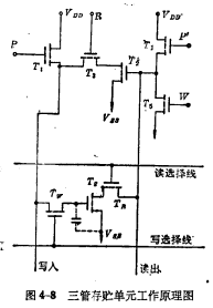
b. Refresh process The refresh process of the circuit is to first read out the information stored in the unit, and then enlarge it by the refresh amplifier. The process of rewriting the unit is as follows:
First add precharge pulse P to make  is turned on to make the write line precharge the image to
  , then repeat the above reading process. The reading process is over, and the reading line appears at a level opposite to the information stored in the cell. The
  tube is controlled by the level on the readout line. If the readout line is "1" level, then
 on, plus refresh control pulse
 , make
 on, the write line will pass
 on, the "0" signal on the write line will be rewritten to the node capacitance
 Up. If the original stored information is "1", the read-out line is "0", so
 At the end, after adding the R pulse, write the data line from
 There is no channel, so the write line maintains the "1" level. When the writing selection line is selected,
 guide Is turned on, the "1" signal is rewritten into the cell and stored in the gate capacitor
 Up. Among them
 is the refresh magnifier. It can be seen from the above analysis that the information is read and amplified, and reversed twice, so the information written in the refresh is exactly in phase with the information in the original memory.
c.Write process First, repeat the above read and refresh process. When the above process is over, give a write pulse W, Ground the readout line, make the refresh amplifier  cut off, and then Send the information to be written into the unit from the write line.
The reading, refreshing and writing of unit storage information are precharged by pulse The selection pulse, refresh control pulse R and write pulse W are controlled. Obviously, these control pulses must maintain strict timing to ensure that the unit works correctly . If the timing of the control pulse is chaotic, the reading and writing will be chaotic, which is a shortcoming of the three-tube unit memory.
(3) Single tube dynamic memory
The number of devices in the single-tube dynamic memory storage unit is the least, so a higher degree of integration can be obtained. Almost all RAMs above 4K bits use single-tube circuits. It is the main form of large-scale and ultra-large-scale RAM development. Figure 4-9 is a partial circuit diagram of a single-tube dynamic memory. The part enclosed by the dashed line is the single-tube storage unit. MOS random access memory ram. It is composed of a MOS tube And capacitance
 composition.
 As a gate control tube to control the entry and exit of data, its gate is connected to the read-write selection line (word line),
 one end is connected to the data line, the other end is connected to the storage capacitor
 The value of should be larger and it should be specially made.
 Is the stray capacitance on the bit line. The reading and writing process of the storage unit is as follows:
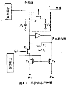
①Write When the row and column decoders are selected, 

 Online data passed
 Controlled by electric charge The form is written into the storage unit.
②After reading out row and column decoder addressing, Turn on, because at this time
 Deadline. Stored in capacitor
 The charge on it passes through the MOS transistor
 Output and charge the stray capacitance O2 on the bit line at the same time. If the capacitance on the bit line
 Small enough and satisfy
 , The readout value is affected by
 The influence of is small, it can be detected by the sense amplifier, through
 Output.
In fact, because of  must be redistributed to
  , which will cause reading Loss at the time of export. Next, we will quantitatively analyze the relationship between the loss of information during readout and the storage capacitance and bit line distributed capacitance.
If the unit storage information "1" level is  , the intermediate level of bit line precharging is
  , then before reading out, in the capacitor
  The charges on the images are
  . After reading, the bit line or the node of the storage capacitor will get a balanced "1" level
 , then on
  The charges are
  . According to the same charge on
  before and after reading, so after reading The balance level of is:

If the information stored in the unit is "0", according to the same principle, the balance level after reading can be written as:

From the two formulas (4-1) (4-2), if  . But the bit line distribution capacitance
  is the same as the number of storage bits in each column In direct proportion, the larger the number of storage bits, the larger the
  . Since the bit line is also connected to a sense amplifier,
  also includes reading Output and input capacitance of the amplifier, so it is impossible to compare
  img src="/userfiles/images/2020/11/16/2020111615316199.png" title="image.png" alt="image.png"/>small. However, in order to minimize the unit area and improve integration,
  No It may be very big. Therefore, the readout voltage will be much lower than the voltage across the storage capacitor, resulting in a very weak readout signal, and the storage capacitor
 is read out, it must be reduced a bit, causing damage to the stored signal. MOS random access memory ram. In order to ensure the normal operation of the memory to read weak signals, there must be a high-sensitivity sense amplifier, and there is a regeneration amplifier in each column to compensate for the corrupted data during reading. Therefore, designing a high-sensitivity regenerative amplifier is the key to a single-tube unit memory.
Like other dynamic memory, the single-tube unit memory must be refreshed. The process is as follows: After the row and column decoders are selected, refresh control pulses are applied  , turn on
  , save it in< img src="/userfiles/images/2020/11/16/2020111615335180.png" title="image.png" alt="image.png"/> The information on the high-sensitivity sense amplifier is amplified, and then
  Rewrite into the storage unit. Figure 4-10 is a schematic diagram of the structure of a single-tube memory cell fabricated by a silicon gate process. It can be seen from the figure that the source diffusion area of the transmission tube is shared with the bit line, and the storage capacitor
  The reaction caused by the silicon shed connected to
  It is composed of type PN junction and silicon gate capacitance. This saves area, increases
  , and reduces Bit line node capacitance.

Contact: Mr. Zou
Tel: 0755-83888366-8022
Mobile: 18123972950
QQ: 2880195519
Address: 5C1, CD Block, Tianji Building, Tian’an Digital City, Chegongmiao, Futian District, Shenzhen
Please search WeChat Official Account: "KIA Semiconductor" or scan the following picture to "Follow" Official WeChat Official Account
Please "Follow" the official WeChat account: provide MOS tube technical assistance


