Electronic Technology Forum
Detailed explanation of the characteristics and working principle of MOS D flip-flop
D trigger features
MOS D flip-flop is an input-side flip-flop. Its characteristic is that the output and input have the same state, regardless of the original state of the flip-flop.
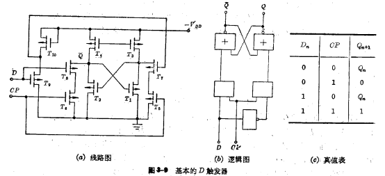
The basic D flip-flop is a temporary information register circuit, as shown in Figure 3-9. It can be seen from the logic logic diagram that the D flip-flop has an inverter added to the front of the RST trigger, and connect the input end of the inverter to the S end of the RS flip-flop; connect its output end (Ie  ) Connect with the R of the RS trigger. It can be seen from the logic diagram that when the D input is "1", the S input of the RS flip-flop is equivalent to "1" and the R input is "0", when the D input is "0" ", which is equivalent to the case where the S terminal input of the RS flip-flop is "0" and the S terminal input is "1". So under the action of
  pulse, the corresponding output Q must be the same as the input The level of terminal D is the same (refer to Figure 3-9
 True value surface). MOS D flip-flop, This kind of basic D flip-flop, although the output is indefinite, and because of the single-ended input, it is more convenient to use, but it has the problem of somersault and does not have the counting function. In MOS circuits, D flip-flops with a master-slave structure are often used. The following introduces several master-slave D flip-flops.

1. The master-slave D trigger changed from the master-slave R-S trigger
Add a level of NOT gate before the master-slave R-S flip-flop mentioned above to form a master-slave D flip-flop. When  is "1" level, the D terminal information is sent first Enter the main trigger storage, and then when the
  is "0" level , The information is transmitted to the output of the slave trigger. MOS D trigger, At the same time, the input of the master trigger is isolated from the outside world. Because
  The output state changes only when it jumps up, so the output is delayed by one clock cycle relative to the input.

This structure of D flip-flop can not only transmit information in a single wire, but also solve the problem of somersaults, so it has been widely used in computers.
2. Master-slave D flip-flop diagram composed of gate control tube
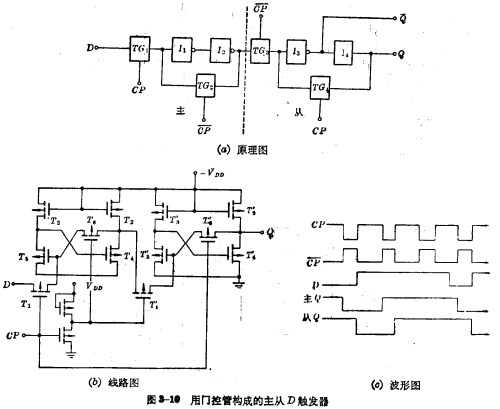
3-10 is a kind of master-slave D flip-flop constructed by gate control. The picture  is the schematic diagram of this trigger. The gate control in the figure is represented by
  , which is subject to
  and
and 
 and
and  Form the main trigger,
  and
and  is formed from the trigger.
  and
and  As the control switch for sending to the master and slave triggers,
  and
and  serves as the feedback gate of the master and slave triggers.
  or
or When turned on, the inverter
  and
and  or
or  and
and  constitutes positive feedback. Because of
  and
and  Sync,
Sync,  sync with
  (They are respectively supported by
  and
and  control), therefore, when the D end passes
  , when the signal is sent to the main trigger, the slave trigger feeds back the original signal from the output terminal to the input terminal to keep it The output state remains unchanged. And the main trigger is due to
 Closed, its status cannot be transmitted to the slave trigger. When
  is turned on, the information in the main trigger is The internal excitation and hold are sent to the slave flip-flop on the one hand, and the information input by the D terminal is obtained at the output terminal. MOS D trigger, also because of
  Turn off, the main flip-flop is isolated from the D input. At this time, no matter how D changes the signal, it will not affect the state in the main flip-flop. So there will be no somersault phenomenon. Figure 3-10 (b) is the circuit diagram of this flip-flop. In the picture
 分别相当于
分别相当于 。The waveform of the entire circuit is shown in Figure 3-10(c). This circuit is different from the various static circuits described above. Although it has the DC storage performance of the AC-coupled flip-flop in the static circuit, the information is temporarily stored by the gate capacitance. Therefore, it’s important to
  and
and  The rising and falling edge requirements are high, otherwise it is likely to cause master-slave competition and make the output state uncertain. At the same time, the frequency of the clock pulse cannot be too low, otherwise, the information will disappear due to the leakage surface. This kind of trigger is also called a quasi-static trigger.

As can be seen from the figure, this circuit structure is relatively simple and saves components.
3, CMOS D flip-flop
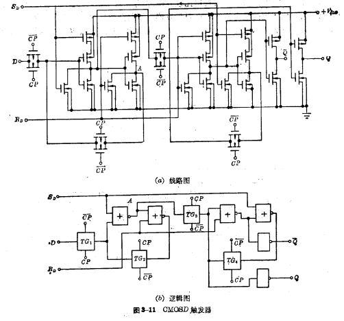
This is a D flip-flop with a complementary quasi-static master-slave structure, as shown in Figure 3-11. It is composed of four NOR gates and four transmission gates. The transmission gate is controlled by the clock pulse  . When the positive clock pulse comes (ie
  ), the transmission gate< img src="/userfiles/images/2020/11/11/2020111115124710.png" title="image.png" alt="image.png"/>Open,
  Closed, there is an A point when the signal from the D terminal enters the main trigger. The original signal from the trigger output is fed back to it through
  Input terminal, so the slave flip-flop keeps the original state. When the negative clock pulse arrives
  , the transmission gate
  Open,
Open, 
 is sent to the output from the trigger; at the same time the signal at point A passes through a NOR gate And
  . MOS D flip-flop, feedback to the input of the first stage NOR gate. Since
  is closed, no matter how the D side changes, the trigger will not be changed status. Where
  、
、 is the reset and set terminal, which has the function of setting and resetting directly. When
  is connected to high potential "1" respectively, the output Q will be Set to 0 or 1, respectively, when the circuit is working,
  is connected 0 potential. The requirements for clock pulses are the same as mentioned above.
Contact: Mr. Zou
Tel: 0755-83888366-8022
Mobile: 18123972950
QQ: 2880195519
Contact address: 5C1, CD Block, Tianji Building, Tian’an Digital City, Chegongmiao, Futian District, Shenzhen
Please search the WeChat official account: "KIA Semiconductor" or scan the picture below to "Follow" the official WeChat official account
Please "follow" the official WeChat account: provide MOS tube technical assistance


