Electronic Technology Forum
Transient response analysis of E/E MOS tube inverter
E/E MOS tube transient response
Transient response is the process of studying the change of the output level with time after the input level of the inverter changes. It is the dynamic characteristic of the inverter. When the input level jumps quickly, we not only need to know the process of the output state changing with the input state, but also whether the output state change can keep up with the input state change. Therefore, it is necessary to study the time from the input state change to the output state flipping process, which is commonly referred to as the output waveform rise, fall and its delay time. The former is the time required for the inverter to turn off and on, also called switching time; E/EMOS transient response, the latter is the time required for the monk to pass the first-level gate, usually described by the average transmission time, this It is an important parameter that characterizes the operating speed of the circuit. The switching time and average transmission time of the inverter will be discussed below.
1. Switching time
The MOS transistor is theoretically a fast switching device, but the actual switching speed of MOS circuits is much slower than the theoretical one. The main reason is that the circuit has a large Parasitic capacitance. Figure 2-19 is a saturated load inverter circuit, with various parasitic capacitances marked on the figure. Where  represents the channel capacitance, gate-source capacitance and wiring capacitance at the input Equivalent capacitance;
  indicates the gate-drain capacitance, source-drain of the output The equivalent capacitance of capacitance and wiring capacitance;
  indicates the next level circuit The input capacitance.
  and
and  is collectively referred to as the load capacitance of the circuit
 Due to the existence of load capacitance, the circuit is in "0", "1" during the transition of the two states, you must correct
  Charge and discharge.
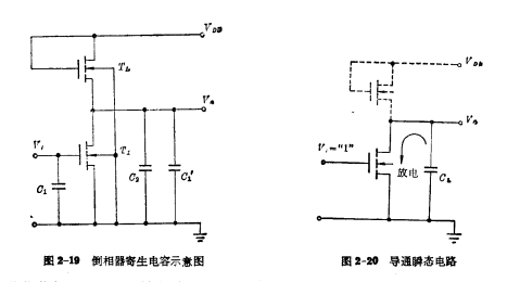
When the inverter inputs the "1" level, the circuit will be turned on from the original cut-off, and the output "0" level. For the circuit to complete such a process, the output load capacitance  must be the original The charge accumulated during the cut-off is discharged through the input tube that has been turned on. Only after the discharge is over, can the potential difference between the two ends of the capacitor
  be close to Zero, that is, output "0" level. As shown in Figure 2-20. E/EMOS transient response, the discharge time for the circuit to complete the above process is called on time, also called fall time. For the convenience of testing, the time required for the output voltage to drop from 90% to 10% of the amplitude is usually defined as the fall time, using
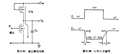
  means, as shown in Figure 2-22.
When the inverter inputs "0" level, the inverter changes from the original on state to the cut-off state, and the output becomes "1" level. It takes a certain amount of time for the circuit to complete such a process. Because the two ends of the output capacitor OL did not accumulate charge, at this time, the output terminal must change from the original "0" to "1", and the capacitor must be adjusted  Charge, so that the two ends gradually accumulate charge to reach the "1" level output. As shown in Figure 2-21. Because the input tube is in the cut-off state at this time, the charging passes through the load tube loop. This charging time is called cut-off time, or rise time. It can be defined as the time required for the output voltage to rise from 10% of the amplitude to 90% as the rise time, which is represented by tr. See Figure 2-22.
(1) Fall time (on time) For the sake of convenience, we can make some approximate assumptions, such as assuming that the input signal is an ideal step wave, because when it is turned on,
  It is mainly discharged through the input tube, and the load current can be ignored, so the load MOS is omitted, and a simplified equivalent circuit of the turn-on instant is obtained. As shown in Figure 2-28. Regardless of whether it is a saturated load or a non-saturated load inverter, it can be handled in this way.
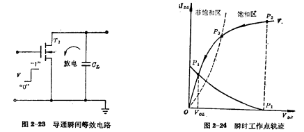
At the moment when the inverter starts to be turned on, that is, the original non-conductive state turns into a fully conductive state. The operating point of the inverter is shown in Figure 2-24. The  jump to
  point. The output of the turn-on inverter should change from "1" level to "0" level. But at this time, the capacitor
  is still the original "1" at both ends Level, then
  Start to discharge through the turned-on input tube to make the output The terminal voltage gradually drops from "1" to "0". During this discharge process, the operating point of the inverter is determined by
  Go through the saturation zone to the point
  , then start from
  The point passes through the unsaturated zone to reach
  point. Therefore, the on-time is composed of two parts, namely the discharge time in the saturated area and the discharge time in the unsaturated area.
①Discharge time in saturation zone
When the output voltage meets , the input tube is saturated, and the transient operating point trajectory corresponds to
  This paragraph. Using the relationship that the capacitor discharge current is equal to the drain-source current of the saturated input tube, the relationship between the switching time and the output voltage can be obtained.
The capacitor discharge current is:
 < /span>
The saturation current of the input tube is:

by  Get the differential equation:

Use the method of separating variables to integrate:

As a result of integration, get the discharge time in the saturation zone:

From the formula (2-31), it can be seen that in the circuit, if the input "1" level is equal to the maximum output high level of the previous inverter , the discharge time in the saturation zone has a minimum value; if you enter "1" The level is less than
  , obviously the discharge time in the saturated zone is longer. Therefore, the value of the input "1" level is different, which has an impact on the rise time.
②Discharge time in unsaturated zone
When the output voltage meets , the input tube works in the unsaturated zone. The transient operating point trajectory corresponds to a section of
  . This section is different from the saturation zone discharge because the capacitor
  is not saturated When the input tube in the zone is discharging, the discharge current gradually tends to zero as the terminal voltage decreases. E/EMOS transient response. Similarly, the differential equation of the relationship between switching time and output voltage can be obtained from the relationship between the discharge current of the capacitor and the unsaturated current of the input tube.
Capacitor discharge current:

Input tube non-saturation current:

Depend on , Get the differential equation:

Solve this differential equation using the method of separating variables:

Use the integral formula:

here, After integration, the discharge time in the unsaturated zone is obtained as:

In summary, when the MOS inverter is turned on, the load capacitance Discharge from the "1" level through the turned-on input tube, and finally reach the "0" level. The total discharge time (that is, the turn-on time of the inverter) should be:

Introduce the equivalent time constant:

Substituting into the formula (2-35), we get:

From the formula (2-36), it is necessary to make the fall time of the inverter Small, be sure to make
  Small, that is, the transconductance of the input tube
 Be sure toto be large. When we export the mathematical expression of
  , although the load management is ignored However, it is more accurate to use (2-36) to calculate the on-time of the inverter, which shows that the simplified analysis result is consistent with the actual situation. In fact, the current of the load tube has an effect on the fall time, but this effect is negligible compared with the total switching time, so in the design, you can use (2-36) to determine the geometric size of the input device.
Here is also to point out that the discharge time in the saturation zone The discharge time is much shorter than that in the unsaturated zone, because in the saturated zone, the discharge current is almost unchanged, which can be regarded as a constant current source discharge; while in the unsaturated zone, with the load capacitance< img src="/userfiles/images/2020/10/30/2020103011452482.png" title="image.png" alt="image.png"/>, the voltage at both ends drops, through
  will become smaller and smaller, so the discharge time in the unsaturated zone will be longer. If you change
  ,
,  The data is substituted into (2-31) and (2-34), which can be calculated as
 Visible,
  , so when actually calculating the fall time of the inverter, the discharge time of the input tube in the saturation zone is often ignored. Therefore, the fall time of the inverter is approximately equal to the discharge time of the input tube in the unsaturated zone.

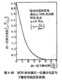
For convenience, you can use the  and the output voltage is written in a normalized form to get the normalized time
 , and normalized output voltage
 Relationship:

According to (2-38) formula, the relationship curve between normalized time and normalized output voltage can be drawn, as shown in Figure 2-25. It can be seen from the figure that the load capacitance  passes through the unsaturated zone of the input tube The discharge time is about
  . In this way, the calculation is a simplified formula.
(2) Rise time (cut-off time)
For the cut-off situation, invertedThe phase device turns from the original conduction to the complete cut-off state at the beginning of the moment . When this, the inverter should output "1" level, for this reason, the load capacitance< img src="/userfiles/images/2020/10/30/2020103011508687.png" title="image.png" alt="image.png"/>Must passThe overload tube is charged to accumulate charge at both ends of the capacitor. E/EMOS transient response, when discussing rising, for convenience, we can ignore the current flowing through the input tube, and the input signal is also assumed It is a step wave. Below, we will discuss the two situations of saturatedload and unsaturated load.
①Saturated load
Same as the method discussed earlier, the load tubethe current  Equal to capacitor current
 (that is, the currents at the output nodes are equal), the differential equation describing the cut-off moment can be obtained. But it must be pointed out that the load tube of the saturated load inverter always works in the saturation region, so the solution is simpler than before.
By solving the differential equation, the rise time of the saturated load MOS inverter can be obtained as:

In the formula is zero, and the final value should be
  .
.
If the equivalent time constant is introduced .
.
A simple function relationship between normalized output voltage and normalized switching time can be obtained:

After transformation, we get:

(2-40) is the function relationship between normalized output voltage and normalized switching time, which can be made 
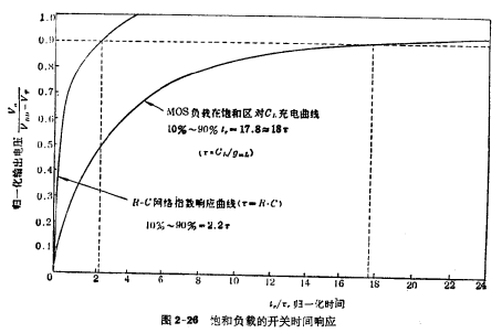
 is shown in Figure 2-26.
It can be seen from Figure 2-26 that the load tube is in the saturation zone. Charging, the time required for the voltage to rise from 10% to 90% is approximately equal to
  . The figure also shows the exponential response curve of the RC network, indicating that the charging time under a fixed resistance is
  . It can be seen that the charging time of the capacitor through the load MOS device is much slower than that of the pure electric anode, and it is also much slower than the discharge time through the input tube, that is, r>sub.
In reality, The starting voltage of is not equal to zero, but at a low level, so the formula (2-39) should be rewritten as:

This style can often be used for design calculations. The rise time calculated from this formula is smaller than  .
.
From the formula (2-39), if you want to reduce  , a high power source must be used
 and high
  , low
, low  value. Because the high
  can obtain a higher charging level, so it is necessary to For the output "1" level,
  The higher the level, the higher Quickly charge to a predetermined level. High
  means a smaller channel equivalent resistance And there is a larger charging current.
②Unsaturated MOS load
The cut-off time of saturated MOS load inverter . The switching speed is abnormally slow, which is mainly due to the load tube working in the saturation zone. The load tube of the non-saturated load MOS inverter always works in the non-saturated region, so the charging speed of the load capacitor is relatively fast. We can use the same method as discussed above to find the cut-off time of the unsaturated MOS load inverter
 .
.
The current in the unsaturated zone is:

 The charging current is:

Depend on , Get the differential equation:

Use the method of separating variables to solve this equation, and use the normalized output voltage and normalized switch time
 , we get:

This is the expression of the function relationship between the normalized output voltage of the unsaturated load and the normalized switching time.
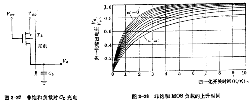
where , Is the bias parameter, the size of m' indicates the depth of the load tube into the unsaturated zone.
 , It is the equivalent time constant of the unsaturated MOS load.
For a known value of the parameter m', it can be made by the formula (2-43)
 , such as m'taking a set of values from 0 to 1, you can get a cluster of curves as shown in Figure 2-28, which can be used for design reference.
 Factor Applicable to the scope of
  , when
  , the formula (2-43) can be simplified to a simple exponential relationship.

This is the case for linear resistive loads. This shows that when Voo-→0o, (m'-0), the load device is already equivalent to a linear resistance, and its switching time is 2.2x. It can be seen that the higher the Voo, the sufficient conduction intention, and the faster the non-saturation zone is charged, the higher the switching speed.
When At the time, you can use the Law of Robida to simplify the formula (2-43) to:

This is the case of saturated load, and its rise time is  . It can be seen that when
  , it indicates the rise time of unsaturated MOS load
 in
in  between. The above analysis did not consider the bias effect of the substrate, such as the bias effect of the substrate, the parameters in the bias parameter and the time constant
 , additional threshold voltage must be added accordingly
 .
.
(3) Maximum operating frequency
Through the discussion on the switching time of the inverter circuit, we can clearly see that for the general circuit, the rise time , much longer than the fall time
 , especially the saturated load MOS inverter, E/EMOS transient response, its rise time is many times larger than the fall time. Therefore, in actual circuit design, the fall time can often be ignored, and only the rise time can be considered. The rise time of the inverter is directly related to the highest operating frequency of the circuit.
Figure 2-29 shows the input and output waveforms of the inverter. It can be seen from Figure 2-29(a) that when the half cycle of the output signal pulse is  , the charging and discharging of the circuit can keep up with the change of the input pulse, and the circuit can work normally. But when
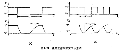
(Figure 2-29(b)), the charging and discharging of the circuit cannot keep up with the change of the input pulse. For example, the input pulse changes from "1" to "0", the inverter changes from on to off, and the load tube pair  Charging, but
  When the charging has not reached the predetermined high level, the level of the input pulse has been converted, and the level of the "0" is changed to the level of "1", forcing the inverter to switch from the cut-off state to the on state. In this way, the amplitude of the output level will drop, and even the output pulse will not reach the value of the gate opening level, and the next-stage circuit will not be normally turned on, and the entire circuit will not work. Therefore, the frequency of the input pulse should be limited by the maximum operating frequency of the circuit.
The so-called maximum operating frequency is when the half period of the input pulse is equal to the rise time of the output pulse , the frequency at which the circuit can maintain normal operation is called the highest operating frequency. By definition:

 为输入脉冲的最小周期。
Therefore, the highest frequency of the circuit is:

2, average transmission time
When the signal is transmitted in the circuit, the output of the front gate is often the input of the rear gate. Therefore, the waveforms of the input pulse and output pulse are no longer ideal step waves. In this way, the rise time and fall time of the output wave will increase, and the delay time of the entire output waveform relative to the input wave is called "transmission time".
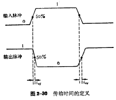
In actual work, for the convenience of testing, a point at 50% of the waveform amplitude is usually taken as the reference point for detecting the time delay between the output voltage signal and the input voltage signal. For the rising edge, the time delay between the 50% of the input pulse and the 50% point of the output pulse is defined as the "rising delay time field", and the falling edge is also defined between the 50% point of the input pulse and the 50% point of the output pulse The time delay is "falling delay time  ", the average transmission time Can be expressed as:

Figure 2-30 shows the definition of transmission time.  and
and  It is also often called pulse delay time,
  refers to the average transmission time of each level of gate circuit, which reflects the circuit transmission signalSpeed. If the gate circuit's
  is larger, the circuit speed will be slower.
From the above analysis, we know that the transmission delay time is different from the switching time, the transmission delay time represents Output signal is behind
the time of the input signal, and the switching time represents the transition time of the output wave.
3. The quality factor of the inverter
As you all know, to increase the switching speed of MOS circuit, try to reduce the rise time r. For saturated negative inverter circuits, reduce
  There are two ways; one is to increase the power supply voltage
 , because a higher power supply can get a higher output voltage
 , in a short period of time, the capacitance
  , can be charged to a predetermined "1" level; another way is to reduce the channel resistance of the load device, that is, reduce the time constant
  , which means to increase the aspect ratio of the load device to increase the charging current. However, the above two points will increase the static power consumption of the circuit
  , but the actual It is always hoped that the power consumption of the circuit should be as small as possible. Therefore, increasing circuit speed and reducing circuit power consumption are contradictory. Therefore, one cannot blindly pursue speed without considering power consumption, nor can it only consider reducing power consumption without considering speed. To evaluate the performance of a circuit, it cannot be measured solely by speed or power consumption. Instead, the product of static power consumption and average transmission time is often used as the merit value to evaluate the performance of the circuit, which is called the quality factor of the circuit, namely:

Unit use joule(
 )。
)。
Contact: Mr. Zou
Tel: 0755-83888366-8022
Mobile: 18123972950
QQ: 2880195519
Address: 5C1, CD Block, Tianji Building, Tian’an Digital City, Chegongmiao, Futian District, Shenzhen
Please search WeChat Official Account: "KIA Semiconductor" or scan the following picture to "Follow" Official WeChat Official Account
Please "Follow" the official WeChat account: provide MOS tube technical assistance


