Electronic Technology Forum
E/E Static characteristic analysis of MOS inverter
1. Discussion of output voltage
From the above analysis, it is known that the inverter has two states of "on" and "off", namely the on state and the off state; the operating point on the output characteristic curve The two voltages corresponding to A and B are output low level and output high level. Use  and
and  means, as shown in the figure Shown in 2-11.
Take a saturated MOS load inverter as an example to discuss the output low level and output high level
 . Figure 2-12 is the equivalent circuit of the inverter.
(1) Output low level
When the inverter is fully turned on, because the on-resistance of the input MOS tube is very small, the output is "0" level, but the actual output voltage is not equal to 0V. Because there is an on-resistance exists, so the actual output voltage should be:

where It is the conduction current when the input MOS tube is turned on.
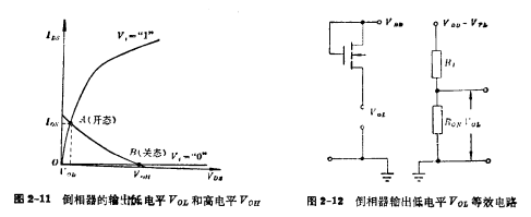
From Figure 2-12 of the equivalent circuit of the inverter, you can write:

where RL is the equivalent resistance of the load MOS tube,  is the current passing through the load tube. Rewrite the formulas (2-5) and (2-6) into the form of electric current, and according to
 , then:

After sorting, get the output low level is:
is:

where Is the on-resistance of the input tube, according to the formula (1-57):

BL is the on-resistance of the load tube, and its value is the on-resistance when it is not saturated 2 times, so there are:

Substituting these two formulas into formula (2-8), we get:

In the design of inverters, often use  , so you can ignore the
  . So get:

You can see,  It is not only related to the process parameters
  , but also related to the load tube and The transconductance of the input tube is proportional. To make the output low level
 close to 0V, it must be designed to meet
  , which is the ratio of
  To be very small. It can be seen directly from Figure 2-13, such as the transconductance of the inverter input tube
 is certain, then the transconductance of the load tube
  the smaller , The inverter output low level
  The closer to the origin; The transconductance of the load tube of the phase converter
  Be sure, then the span of the input tube The larger the guide, the lower the output
  will be closer to the origin.
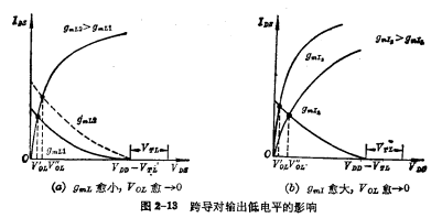
As mentioned earlier, the size of transconductance directly reflects the W/L ratio of the device channel.  The larger the channel, the larger the channel's aspect ratio, and vice versa.
  The smaller the channel, the smaller the channel's aspect ratio. Therefore, to make the output low level of the inverter close to 0V, the size of the input tube should be much larger than the size of the load tube when designing. According to the calculation formula expressed by the formula (2-9), the design can be directly carried out.
(2) Output high level
When the inverter is cut off, the cut-off resistance of the input tube is very large, most of the power supply voltage falls on the cut-off resistance of the input tube, and the output is high. . Since the inverter is in the cut-off state at this time,
 ,which is:

Therefore, the maximum value of the output high level is obtained as  , It can be seen that the output high level is only related to the valve voltage of the load tube
 Related. Due to the influence of the back gate effect, the load tube
 It varies with the output voltage. So calculate
 It’s more complicated. In the actual design, generally determine the output high level first
 the value, and then calculate< img src="http://www.kiamos.cn/userfiles/images/2020/10/29/2020102910529085.png" title="image.png" alt="image.png" style="font-size: 18px ; white-space: normal;"/>, then determine the power supply voltage
 。
。
Considering the backside gate effect, output high level V. The expressions for outputting and outputting low-level VaL should be changed accordingly. ie:

2. Voltage transmission characteristic curve
MOS inverter output voltage and input voltage
  The relationship is called the voltage transfer characteristic. Figure 2-14 is a schematic diagram of the voltage transmission characteristic curve of the inverter.
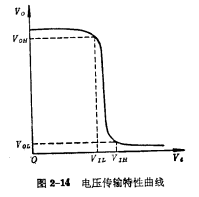
As seen from the figure, when the input signal of the inverter is less than or equal to  , the inverter is cut off and the output is high
 ; when the input signal is greater than
  , the inverter is turned on and outputs low level
 ; When input signal
  in
in  and
and  , the inverter is in the transition zone between on and off.
The voltage transmission characteristic curve of a specific MOS inverter can be measured point by point for each input voltage The corresponding output voltage
 , and get it by drawing, or it can be displayed directly by the graphic instrument. The following will analyze the transmission characteristics of saturated negative I and non-saturated load inverters.
(1) Transmission characteristics of saturated MOS load inverter
In this kind of inverter, the load tube always works in the saturated zone, and the input tube can work in the saturated zone or the unsaturated zone according to different working conditions. Area. If  , the input tube works in the saturation zone; if
  , the input tube works in the unsaturated zone. Here
  is the threshold voltage of the input tube,
  . For the convenience of discussion, the back gate effect is not considered first, so VTL=VTI=VT. Below, we start from the current formula to derive the mathematical expression of the voltage transmission characteristics, and make a normalized transmission characteristic curve.
When the load tube and the input tube are in saturation, the current expression is:


Because the current through the two tubes of the inverter is equal ( ), that is:

Among them
The maximum output voltage for the above type For normalization, you have to:

It is easy to see that this is a straight line equation, namely  With
With The change is approximately linear. Pair (2-18) type
  Find the derivative, and the slope of the line is:

So I get:

It can be seen that the formula (2-15) has nothing to do with the applied voltage, but only with the geometric size of the device. Therefore, if you get it theoretically,  The value of the input device and The geometric size ratio of the load device. When the load tube is working in the saturated zone and the input tube is working in the non-saturated zone, the current can be written as:

Since the current through the two tubes of the inverter is equal,  , you can get the
  relationship Equation:

Mix the above formula to the maximum output voltage is normalized to get:

It is not difficult to see that this is a curve equation, namely  Following the changes of
  Non-linear relationship.
Equations (2-13) and (2-16) reflect the functional relationship between the normalized output voltage and the input voltage. For the coefficient  can normalize the output voltage in various situations< img src="/userfiles/images/2020/10/29/2020102911387119.png" title="image.png" alt="image.png"/>
 and normalized input voltage
 The relationship curve is drawn.
Normalized input voltage cloud number if parameter Taking seven values of 4, 9, 16, 25, 86, 49, 64, seven voltage transmission characteristic curves can be made. E/E MOS static characteristic analysis, as shown in Figure 2-15.
As can be seen from the picture:
①Saturated MOS load inverter output high level, the maximum value is  ;
;
② Increasing the value makes the transmission curve steeper, the output "0" level is closer to 0V, and the voltage transmission characteristics are better.
The actual inverter design is based on the requirement of the output “0” level in the case of input “1” level, and the conductivity factor is obtained from Figure 2-15. Ratio βR, then calculate the ratio of the width to length ratio of the two devices, and finally determine the size of the device. So Figure 2-15 is also called proportional design curve, which is very useful for inverter design.
For example, design a common-gate-drain MOS inverter, its power supply , design requirements
 . When
  ,
,  , find the inverter's
 . Assume that the resistivity of the silicon chip is
Solution a. Calculation of load tube The load tube can be calculated according to the requirements of power consumption.
Static power consumption of the inverter , the current in the power consumption expression is the current when the inverter is turned on under saturated load conditions, that is, the maximum quiescent current
 , ie:
, ie:

In the formula Equal to the drain-source voltage of the load tube. If the inverter output low level is close to zero volts, then
  ; In the formula
  is integrated Under the conditions, it should be
  . The effect of the backside shed effect is not considered here. , Still use
  . So:
. So:

So I get:

Because of:


Get:

The load device (W/L) z obtained here is the maximum value.
b. Input MOS tube calculation Generally, input MOS tube is considered according to the requirement of inverter output low level. In order to apply the design curve shown in Figure 2-15, the normalized output voltage and input voltage need to be calculated first.

Check image 2-15, get  , ie:
, ie:

So:

Preferable:

Of course, theoretical calculations point us out a direction. In actual design calculations, we need to modify them according to specific conditions. value to get a satisfactory circuit device size.
(2) Transmission characteristics of unsaturated MOS load inverter
Similar to the analysis method of saturated MOS load, the load tube that flows through the unsaturated zone can be obtained first. The current expression. Because of:

So:
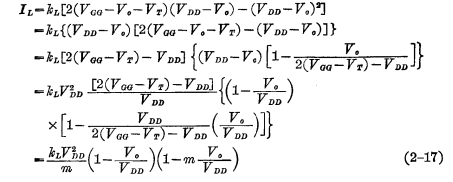
where:

m is called the bias parameter, which indicates the depth of the load tube into the unsaturated zone. It can be seen from equation (2-18) that the larger the value of m, the closer to saturation. When m=1, it just starts to be saturated, and the smaller the m, the deeper the degree of saturation. So the range of m value is 0<m<1. Let’s analyze the input MOS tube. When When, T< span style="font-size: 10px;">Iwork in the saturated zone, so:

When When, TI works in the unsaturated zone, so:

Because it flows through TI and T The currents of L are equal, so when TI works in the saturation zone, there is:

TI working in the unsaturated zone, there are:

Make some transformations in (2-21) and (2-22), then TI In the saturation zone  and
and  The relationship between:

This is the transmission characteristic equation of the unsaturated MOS load inverter when the input tube is working in the saturation region,  With
With is approximately linear. TIIn In the unsaturated zone,
 and
and < span style="font-size: 18px;">The relationship is:

This is the transmission characteristic equation of the unsaturated MOS load inverter when the input tube is working in the unsaturated region,  With
With shows a non-linear relationship. E/E MOS static characteristics analysis
Using formula (2-23) and formula (2-24), for different m values, unsaturated MOS load inverters with m values ranging from 0.1 to 0.9 can be made The normalized theoretical transmission characteristic curve (Figure 2-16). These curves can be used for design.
The method of use will be briefly described as follows:
①First determine the value of the offset parameter m (reflecting the unsaturated depth).
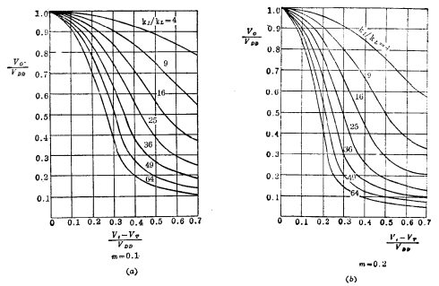
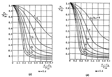
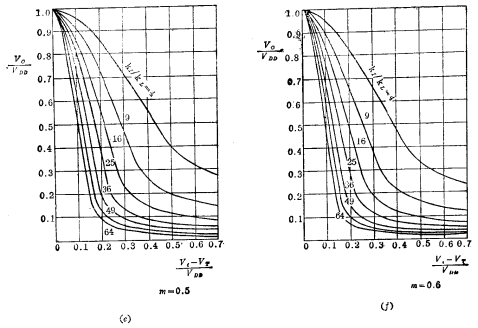
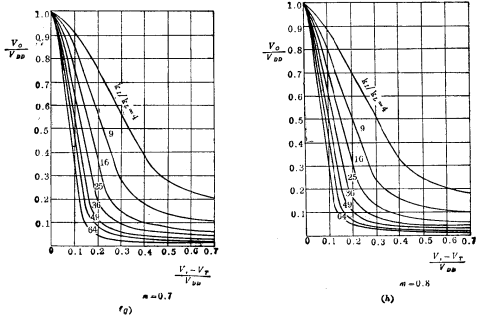
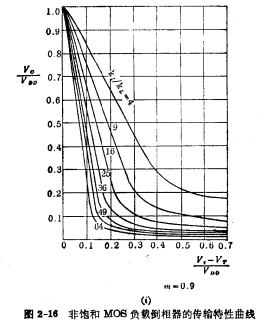
②Determine the values of normalized output voltage and normalized input voltage, and find the corresponding  value.
③Re-check the  value to determine the device's aspect ratio W/L. E/E MOS static characteristics analysis
3. Noise tolerance
The so-called "noise tolerance" refers to the maximum noise voltage that the input terminal can withstand without destroying the normal working state of the circuit. It characterizes the size of the circuit's anti-interference ability. That is to say, when there is a parasitic signal (interference voltage) at the input, the circuit can guarantee the ability of normal output. The noise tolerance of the inverter can be estimated from the voltage transmission characteristic curve, as shown in Figure 2-17.
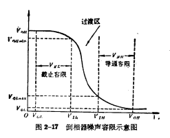
In the picture Is called the door closing level, and
  is the door opening level. The so-called closing level refers to the minimum value of the output high level when the circuit is in critical cut-off
 The corresponding input level; the so-called gate opening level refers to the maximum output low level when the circuit is in critical conduction
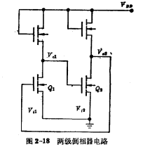
The following is an example of a two-level interconnected common-gate drain load MOS inverter circuit (see Figure 2-18) to illustrate the size of the noise margin.
If the size of the load device and the input device of the two-stage inverter are the same, their threshold voltage VT is also the same, so the transmission characteristic curves of the two-stage inverters are exactly the same. It can be seen from Figure 2-18 that if the circuit is to output the "1" level, the second-stage inverter Q2 is required to be reliably cut off Status, you must require input low level  . And the input low level
  is the output of the first-stage inverter Low level
  and noise voltage
 , so
, so 
 , that is,
  , it will destroy the second-stage inverter Q2 The cut-off state of makes the circuit work abnormally. It can be seen that the interference voltage value that destroys the cut-off of the second-stage inverter is
  . Therefore, the noise margin of the second-stage inverter cut-off is
  .
.
If the first-stage inverter Q1 can be reliably and fully turned on, it must be required The input "1" level  , and
, and  is the "1" level normally output by the second-stage inverter. Due to the interference signal, the signal input to the first-stage inverter
 may be reduced to make
  . Therefore, the condition to ensure the reliable conduction of the first-stage inverter is:
 , and when
 , it may damage the first-stage inverter Q1 normal work. It can be seen that the interference voltage value that prevents the inverter from turning on reliably is:
 . Therefore, the conduction tolerance of the first-stage inverter is:

After the above analysis, we can get the definition of the inverter's cut-off tolerance and turn-on tolerance (see Figure 2-17).
Cut-off tolerance (also called input low-level noise tolerance) . When the input is low, the maximum allowable input noise voltage to ensure that the circuit does not damage the cut-off state is the door-closing level
 and output low level
 Difference:

 Heal Larger, the stronger the low-level anti-interference ability of the circuit.
Continuity tolerance (also called input high-level noise tolerance) . When the input is high, the maximum allowable input noise voltage to ensure that the circuit does not damage the conduction is the output high level
 and door opening level
 Difference:

 Heal Larger, the stronger the high-level anti-interference ability of the circuit.
It can be seen that in order to make the circuit have a strong anti-interference ability, it must have a low 
 Small, must be guaranteed in the design
  . Usually take the inverter's
  in the range of 10-20 times, if If this value is too small, the noise margin of the circuit will be small, and the anti-interference ability will become worse. In addition, to make the circuit have good anti-interference ability, the valve voltage
 The size of the image should be controlled appropriately; use a higher power source
 , Improve
  , which is beneficial to improve the anti-interference ability. E/E MOS static characteristics analysis
Tel: 0755-83888366-8022
Mobile: 18123972950
QQ: 2880195519
Address: 5C1, CD Block, Tianji Building, Tian’an Digital City, Chegongmiao, Futian District, Shenzhen
Please search WeChat Official Account: "KIA Semiconductor" or scan the following picture to "Follow" Official WeChat Official Account
Please "Follow" the official WeChat account: provide MOS tube technical assistance


