Electronic Technology Forum
The working principle of E/EMOS inverter and the influence of inverter performance
E/EMOS inverter working principle
1. Working principle
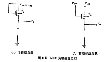
In the E/EMOS inverter circuit, the load tube usually has two bias states. One is the gate-drain common connection power supply VDD, called saturated MOS load; the other is the gate single connection power supply , Called the unsaturated MOS load. The connection methods of these two load MOS transistors are shown in Figure 2-5. The working principles of these two inverters are discussed below.

1. Saturated MOS load inverter
(1) I-V characteristics of the load tube
In Figure 2-5(a), TL is a MOS load device with a common gate-drain connection. It is different from the pure resistive load mentioned above. A variable resistor that changes with the source voltage. due to VDD= ,VDS
,VDS , So it meets
  . Therefore, it always works in the saturation zone. In addition, we can see that the source voltage Vs of the load tube changes,Therefore, the gate bias voltage VGS will also change, and the channel resistance will also change. This is the gate bias voltage VGS is modulated by the source voltage VS.Figure 2-6(a) shows
  .
.
When the source voltage of the load MOS transistor  increases, it will cause a gate The source voltage VGS becomes smaller, which makes the channel thinner and the channel resistance increases, so the current Ios also gradually decreases. Figure 2-6(b) is the I-V characteristic curve of a common-gate-drain MOS load. It can be seen that when Vs=0,VDDThe largest, so Im is also the largest. When Vs increases, VGS becomes smaller, and Ios gradually decreases; when a increases to equal VDD-VT, then VGS-VT, the load tube is in the micro-conduction state, so IDS≈0。
From the IV characteristic curve of the total leakage negative I tube, it can be seen that its IV characteristic is a curve, indicating that the load tube is a variable resistor. When Vs changes from 0V to VDD-VT, the resistance value becomes larger and larger.
(2) Inverter operating point
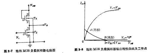
The principle of phase inversion of the saturated load MOS inverter is the same as the principle of the above-mentioned resistive load inverter. When inputting "1" level ( ), input MOS tube guide Pass. In fact, the load tube is also on at this time, but the on-resistance of the sub-input tube is designed to be much smaller than the on-resistance of the load tube. The power supply voltage is V DD mostly land on the load tube TL, so the output voltage is "0" level.
When the input is "0" level, the input MOS tube  is completely cut off , Its cut-off resistance is very large, and most of the power supply voltage falls on
 , So the output is "1" level. At this time, the
  on the load tube is in a micro-conduction state. The two output characteristic curves of the input tube cut-off and on-state are shown in Fig. 2-8. For example, the IV character curve of the load tube (that is, the load line) and the two output characteristic curves of the input tube are superimposed to obtain the output characteristic curve of the inverter and two operating points A and B, where A is the open state The operating point indicates the on-state of the inverter and outputs "0" level; B is the off-state operating point, which indicates the off-state of the inverter, and outputs "1" level.

In summary, the saturated MOS inverter only uses one power source, has a relatively simple structure and is more convenient to use. But because the maximum output voltage can only reach VDD-VTL, The voltage is lower than the value of the voltage by one circle, and VS is not directly grounded, due to the backside gate effect, VT The value should be increased to reduce the output voltage amplitude. If it is required to output a higher high level. It is necessary to increase the power supply voltage, resulting in unnecessary power loss; moreover, because the load tube works in the saturation region, when the output is close to the high level value, the load tube is close to the cut-off state, and the resistance becomes very large, which is not good for the circuit speed. This will be analyzed below.
2、Unsaturated MOS phase detector
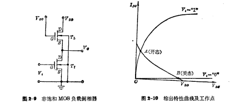
As mentioned above, although the saturated load MOS inverter has a simple structure, it has obvious shortcomings. In order to improve the performance of the inverter and increase the output voltage amplitude and working speed, the grid of the load tube of the inverter can be connected to a power supply VGS, Make the load tube work in the unsaturated zone. This kind of inverter is called a non-saturated load MOS inverter, as shown in Figure 2-9.
In order to make the load tube work in the unsaturated zone, it must meet:

due to:

因此:

即

这就是说,要使负载管工作在非饱区, 的取值至少要比VDD高一个阀值电压

与前面分析饱和负载MOS倒相器的方法相同,将负载管的I-V特性与输入管导通、截止两个状态的输出特性迭加起来,就得到倒相器的输出特性曲线和两个工作点A和B。如图2-10所示。A为开态工作点;B为关态工作点。由于负载管始终工作在非饱和区,沟道电阻很小, ,所以输出高电平近似等于VDD。
综上所述,非饱和MOS负载倒相器有以下的特点:负载管始终工作在非饱和区,阻值较小,有利于提高工作速度;输出摆幅较大,最大输出电压可达到电源电压VDD;但由于增加一个电源,增加了线路结构的复杂性;况且功耗较大,输出低电平的数值稍有提高。
联系方式:邹先生
联系电话:0755-83888366-8022
手机:18123972950
QQ:2880195519
联系地址:深圳市福田区车公庙天安数码城天吉大厦CD座5C1
请搜微信公众号:“KIA半导体”或扫一扫下图“关注”官方微信公众号
请“关注”官方微信公众号:提供 MOS管 技术帮助


