Electronic Technology Forum
The working principle of resistive load MOS inverter and the influence of inverter performance
MOS integrated circuits are currently widely used and have many varieties, and many large-scale integrated circuits with complex functions have been developed. Although various specific logic circuits have different functions and have their own particularities, they can decompose any complex MOS circuit into the most basic inverter circuit. Resistive load MOS tube. Therefore, a clear analysis of the principle and characteristics of the inverter can solve the common problems encountered in the circuit design.
MOS inverters can be divided into four types according to the circuit structure and manufacturing process.
①Resistive load MOS inverter this kind of inverter
Its input tube is an enhanced MOS tube, and the load is a linear resistor.
②E/EMOS inverter this kind of inverter
The input device and load device are both enhanced MOS tubes, called enhanced-enhanced MOS inverters. According to different channels, it can be divided into PMOS and NMOS inverters.
③E/DMOS inverter this kind of inverter
The input device is an enhanced MOS tube, and the load device is a depleted MOS tube, so it is called an enhanced-depleted MOS inverter. This kind of inverters, mostly N-channel devices, can also be manufactured with P-channels.
④CMOS inverter
It is composed of two MOS tubes with different channels in series. Either an enhanced NMOS tube is used as an input device and PMOS is used as a load, or an enhanced PMOS is used as an input device and an NMOS is used as a load. This kind of inverter is called a complementary inverter.
These four inverters have a common feature, and their input devices are all enhanced MOS transistors.
This chapter mainly describes the working principles of E/EMOS, E/DMOS, and CMOS inverters and the gate circuits composed of these inverters.
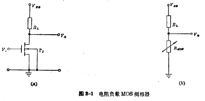
Figure 2-1 is an inverter circuit with resistor RL as the load. Its input tube is an N-channel enhanced MOS tube ,The load is a pure resistance RL. Resistive load MOS tube. The source of the input tube is grounded, and one end of the load resistance RL is connected to the drain of the tube, and the other end is connected to the power supply VDD.Use the gate of the input tube as the input terminal, and use the input signal
  (ie VGS) means that the output terminal is taken out from the junction of the drain and resistance, and the output signal is used
 (Ie VDS) means.

1. Working principle of resistive load MOS inverter
Let's explain how it works. When inputting the "1" level, for example,  , because
 , So the input MOS tube is fully turned on. Since the on-resistance of the MOS tube is much smaller than the load resistance RL, the voltage drop on the MOS tube is very small, that is, the output "0" level (
 ). Conversely, if the input is "0" level (grounded),Because
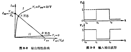
  , the input MOS tube is cut off, and the channel resistance is much higher than pure resistance RL is large, so the output becomes "1" level (V.≈ VDD ). The two states of the input MOS can be represented by the two output characteristic curves of the MOS tube in Figure 2-2. Resistive load MOS tube. Among them, a straight line close to the voltage coordinate axis represents the output characteristic curve when the input MOS tube is turned off, and the upper line represents the output characteristic curve when the input MOS tube is turned on. Figure 2-3 shows the corresponding relationship between the input and output waveforms of the inverter, indicating that the inverter has the function of phase inversion.

2. Load line and working point
The so-called load line refers to the functional relationship between the output voltage Vo of the inverter and the working current IDS. When the input device is fully turned on, the voltage drop on the inverter load resistance is:

Since the output voltage at this time is  =0, soIDSRL=VDD. therefore:

If  , the input tube is in cut-off state , That is, IDS≈0, so:

Therefore, according to (2-2) and (2-3), two points can be made on the coordinate axis of the output characteristic curve, one point is 
 A straight line connecting these two points is the load line of the inverter. It intersects the output characteristic curve of the input tube at two points A and B, which are the two operating points where the inverter is on and off.
Point A is the on state of the inverter, and point B is the off state of the inverter. The voltage Vo corresponding to the two points A and B is the output low and high level. It can be seen from the figure that the output voltage range is approximately 0~VDD; it can be seen that the output voltage swing of the resistive load inverter is comparative big.
Three, the impact of different loads on the performance of the inverter
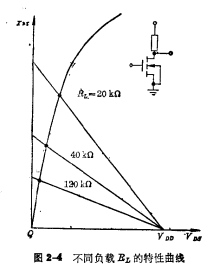
The relationship between the performance of the inverter and the value of the load RL can be shown in Figure 2-4. The figure shows the output characteristic curve of different inverters with load resistance RL. It is obvious from this curve that when RL increases, the load line approaches the horizontal axis, and the open-state operating point approaches the origin, making the output " The 0" level is closer to 0V, and the operating current of the inverter is also smaller, which is what we hope. Because practical applications always hope that the output "0" level is as close to 0V as possible, and the power consumption of the inverter is also as small as possible. It can be seen from the figure that RL=120kΩ is better than RL=20kΩ The inverter performance is much better, RL less than 20kΩ is not practical.

In fact, it is difficult to manufacture an integrated MOS circuit with an inverter that uses a resistor as a load device. Resistive load MOS tube. Because there are certain problems with the use of diffused resistors or thin film resistors. Resistive load MOS inverter
There are three disadvantages when using diffused resistance as a load:
①Use diffusion technology to make high-resistance resistors with low yield;
②It occupies a large chip area and cannot improve the integration level;
③The area of the diffused resistor is large, and the distributed capacitance between the diffused junction and the substrate is also large, which affects the switching speed of the circuit.
So in MOS integrated circuits, a pure resistance is generally not used as a load, but a MOS tube is used as a load, which is called a load tube.
Contact: Mr. Zou
Contact number:0755-83888366-8022
Mobile phone:18123972950
QQ:2880195519
Contact Address: 5C1, Block CD, Tianji Building, Tianan Digital City, Chegongmiao, Futian District, Shenzhen
Please search WeChat official account: "KIA Semiconductor" or scan the following picture to "Follow" official WeChat official account
Please "follow" the official WeChat account: provide MOS tube technical assistance


