Electronic Technology Forum
MOS transistor graphic design example structure detailed analysis
MOS transistor version graphic design example
MOS transistor graphics design, manufacturing MOS transistors, first of all, according to the given parameters, design a pattern that meets the requirements. Here is a brief introduction to design a MOS transistor pattern according to the requirements of transconductance gm.
When set threshold voltage ,Transconductance of the tube required gm=
 。
。
According to the conditions, the designed MOS transistor is an N-channel enhancement type device, and the given ga is the saturation region transconductance. The graphic design here comes down to determining the width-to-length ratio of the device channel 。
。
According to the transconductance formula in the saturation region:


The aspect ratio of the device can be written as:

If take:
Obtainable:
Substituting the above values, the width-to-length ratio of the device is calculated as:

If the channel length L is 8 μm, then W is 64 μm.
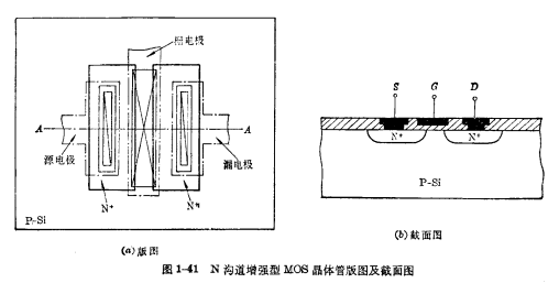
Therefore, according to the determined aspect ratio, the layout shown in Figure 1-41 (a) can be drawn. In the graphic design of MOS transistors, the large square represents the substrate P-Si, and the two long squares on the left and right represent the drain-source N+ area. The gap in the middle is the width and length of the channel. Oxide layer; dotted lines indicate aluminum leads; diagonal lines indicate lead holes. If you cut along the dotted line AA, you can get a cross-sectional view as shown in Figure 1-41 (b).
Contact: Mr. Zou
Contact number:0755-83888366-8022
Mobile phone:18123972950
QQ:2880195519
Contact Address: 5C1, Block CD, Tianji Building, Tianan Digital City, Chegongmiao, Futian District, Shenzhen
Please search WeChat official account: "KIA Semiconductor" or scan the following picture to "Follow" official WeChat official account
Please "follow" the official WeChat account: provide MOS tube technical assistance


