Electronic Technology Forum
What is the highest frequency of the MOS tube and the frequency characteristics of the MOS tube
The highest frequency characteristic of MOS tube
After the frequency of the MOS tube increases to a certain value, its characteristics will deteriorate as the frequency increases. As we all know, the channel region of the MOS tube is separated by an insulating oxide layer, and the metal gate electrode is covered on this oxide layer, so a flat capacitor with oxide as the medium is formed, called the gate capacitance, with the symbol  means.If the change of the input signal at a certain moment causes the increase of
  The carriers induced in the road will increase. The increasing process of these induced carriers is the charging process of the gate capacitance.Charging is carried out through the on-resistance of the MOS tube
  ,The charging time constant is
  and when the VG decreases,
 It must be discharged through
  .
.
When the period of the input signal is greater than the gate capacitance through  The time constant of charge and discharge For a long time (low frequency condition), the charging and discharging process of the gate capacitance is fully carried out, and the output signal can fully keep up with the change of the input signal. The frequency of the MOS tube. At this time, the amplification performance of the MOS tube will not be affected. However, when the period of the input signal is smaller than the time constant for charging and discharging the gate capacitance,That is, the angular frequency of the input signal
  is higher than the natural frequency of the MOS tube Hour,That is,
  . In this way, the charging and discharging process of the gate capacitance is not sufficiently performed, and the output signal cannot completely keep up with the change of the input signal. At this time, the amplification characteristics of the MOS tube will deteriorate.
When the angular frequency of the input signal  , we define The frequency at this time is the highest frequency of the MOS tube, expressed by fm.

Because  , the above formula can be rewritten as:

Where  is the capacitance of the parallel plate capacitor,Can be written approximately as
 .
. is the oxide layer capacitance per unit area.A is the channel area under the gate. So
 can be written as:

Substituting  into the formula (1-68):

This is the expression of the highest operating frequency of the MOS tube. Here  is an oxide layer capacitor
 Substituted, the actual
  will change its size as VGS changes .
It can be seen from the formula (1-69) that the frequency of the MOS tube, the highest frequency of the MOS tube, is inversely proportional to the square of the channel length. It can be seen that in order to increase the maximum frequency of the MOS tube, the channel length L must be designed to be shorter. in addition, It is proportional to
  . Because the electron mobility is greater than the hole mobility, under the same other conditions, the high-frequency performance of the N-channel MOS tube is better than that of the P-channel MOS tube.In order to have a quantitative concept of
  , an example is given below.
If the of an N-channel MOS device can be calculated as:


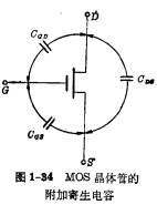
This is a relatively high frequency device. In fact, the frequency of the MOS tube, the highest frequency of the tube in the MOS circuit, is at least 2 to 3 orders of magnitude lower. This is because there are many parasitic capacitances. Among them is the gate-source coverage capacitance caused by the overlap of the metal gate and the source diffusion region (including distributed capacitance between leads), additional parasitic capacitance between gate and drain
 ;In addition, there are the PN junction capacitance between the drain and the P-type substrate and other parasitic capacitances, which will constitute the additional parasitic capacitance between the drain and the source.
 . These capacitors are attached to the MOS tube (as shown in Figure 1-34), which will further deteriorate the frequency characteristics of the device.

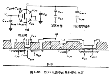
In MOS integrated circuits, in addition to the capacitance of the MOS tube, there are other parasitic capacitances of the MOS tube shown in Figure 1-35, which play a great role in the circuit. This is the reason why the speed of MOS integrated circuit is low and the capacitor is encrypted. Figure 1-35 shows a schematic diagram of various parasitic capacitances in MOS integrated circuits, where:
 MOS trench capacitance;
 PN junction capacitance;
 :Metal-covered oxide capacitor;
 Metal-thin oxide layer-N area capacitor;
 Metal-thick oxide layer-N-zone capacitance.

Contact: Mr. Zou
Contact number:0755-83888366-8022
Mobile phone:18123972950
QQ:2880195519
Contact Address: 5C1, Block CD, Tianji Building, Tianan Digital City, Chegongmiao, Futian District, Shenzhen
Please search WeChat official account: "KIA Semiconductor" or scan the following picture to "Follow" official WeChat official account
Please "follow" the official WeChat account: provide MOS tube technical assistance


