Electronic Technology Forum
The main parameters of the MOS tube and the low-frequency small signal parameters of the MOS tube
As we all know, when any device works at a higher frequency, the capacitance of the device will play a significant role. What is considered here is that when working at low frequencies, the capacitance effect of the MOS tube is negligible, and the input signal is small. The parameters discussed in this case are called low-frequency small-signal parameters.
1、Transconductance of MOS tubegm
The transconductance of the MOS tube is defined as the rate of change of the drain-source current with the gate-source voltage when the drain-source voltage is constant. MOS tube low-frequency small signal. In other words, when the gate-source input voltage changes by 1V, the drain-source current changes. Therefore, transconductance is a physical quantity that characterizes the sensitivity of the gate voltage control output current change. The larger the transconductance, the stronger the control ability. The unit of transconductance is Siemens, and the symbol is S (A/V). Its mathematical expression is:

Substituting the current formula of the non-saturated region of the N-channel MOS tube into the above formula, we get:

It shows that the transconductance of the unsaturated zone increases with the increase of VDS. When VDS is constant, gm has nothing to do with VGS. MOS tube low-frequency small signal. But in fact k is related to VGS. Therefore, as VGS increases, gm will appear to decrease.
Substituting the leakage current formula of the saturation region of the NMOS transistor into the equation (1-54), the transconductance of the saturation region can be obtained as:

Comparing equations (1-56) with equations (1-50), it can be seen that the transconductance of the saturated region is exactly the reciprocal of the on-resistance of the unsaturated region under the same gate voltage, namely:

This is a very important relationship and will be used frequently below.
It can be seen from equation (1-56) that the transconductance gm of the saturation region is related to the channel length L and the gate oxide thickness. It is inversely proportional and directly proportional to the channel width W. If the gate oxide thickness  is constant, the size of the transconductance is determined by W/L. In order to increase the transconductance, it is necessary to use
 Smaller. Therefore, in the manufacturing process of the MOS tube, attention must be paid to the control of the thickness of the gate oxide layer.

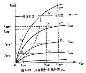
The size of a MOS tube gm can be solved from the saturation region on the output characteristic curve. MOS tube low-frequency small signal. It can be seen from Figure 1-32 that the transconductance of the saturation region has nothing to do with VDS, but increases with the increase of (VGS-VT). For different VGS, gm is different.The transconductance near the grid voltage  can be calculated according to the definition, That is:

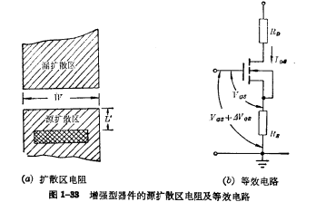
Finally, it must be pointed out that the transconductance will also be affected by the source series resistance Impact,When
  is large, the impact on the transconductance of the device cannot be ignored. The original transconductance of the device will be reduced. mos tube low frequency small signal,
Assume that the transconductance of the original device is If the input signal VGS has an increment
 Then the current flowing through the tube must increase
 . MOS tube low-frequency small signal.In the input loop of the equivalent circuit in Figure 1-38, this increment can be considered
 respectively land on the channel and source series resistance Rs, namely:

Organize the above formula:

which is:

From the formula (1-59), if Rs is small, then When Rs is larger, transconductance will drop a lot. Therefore, in order to reduce the influence of source diffusion resistance on transconductance, Rs should be reduced as much as possible.
The source diffusion resistance can be calculated by the following formula:

2、Drain-source output conductance GDS and dynamic resistance
(1)Drain-source output conductance
When the source voltage is constant, the rate of change of the drain-source current with the drain-source voltage is called the conductance of the MOS tube . mos tube low frequency small signal,It is used to characterize the control ability of output voltage to output current, using means, its mathematical expression is:


The unit of gDS is still Siemens (S).
(2)Drain-source dynamic resistance
The reciprocal of the drain-source output conductance is called the drain-source dynamic resistance. Use  Indicates that this is another important parameter in MOS circuit design, and its unit is ohm. The mathematical expression is:

As mentioned before, in the saturation region, the drain-source current does not change with the drain-source voltage due to the channel pinching off, so the dynamic resistance should be infinite, that is:

In fact, as VDS increases, IDS increases slightly. MOS tube low-frequency small signal. Therefore, the dynamic resistance of the saturation zone is not really infinite, but tends to a finite value, generally in the range of 10~100kΩ.
In the unsaturated zone, the sub-VDS is very small and the channel is not pinched off. It can be considered that the thickness of the channel is similar everywhere. Therefore, the dynamic resistance of the unsaturated zone can be approximately equal to the DC on-resistance:

3、Voltage amplification factorKv
Voltage amplification factor is used to describe the rate of change of drain-source output voltage caused by the change of gate-source input voltage, expressed by Kv:

After transformation, we can get:

It can be seen that the voltage amplification factor is proportional to the transconductance, and the greater the transconductance, the better the amplification performance. According to theoretical analysis, the dynamic resistance in the saturation zone  tends to infinity, so the voltage The magnification factor should also tend to infinity. But in fact, the dynamic resistance in the saturation zone is not really infinite, but a finite value, so the voltage amplification factor is also limited.
In the unsaturated zone (VDS→0), the voltage amplification factor is:

Contact: Mr. Zou
Contact number:0755-83888366-8022
Mobile phone:18123972950
QQ:2880195519
Contact Address: 5C1, Block CD, Tianji Building, Tianan Digital City, Chegongmiao, Futian District, Shenzhen
Please search WeChat official account: "KIA Semiconductor" or scan the following picture to "Follow" official WeChat official account
Please "follow" the official WeChat account: provide MOS tube technical assistance


