Electronic Technology Forum
Structural characteristics and working principles of MOS field effect transistors
MOS integrated circuits are basically composed of MOS transistors, so MOS transistors are the basis of MOS integrated circuits. Before discussing MOS circuits, we must have an in-depth understanding of the principles, basic characteristics and various parameters of MOS transistors.
This chapter mainly describes the physical basis, basic characteristics and main parameters of MOS field effect transistors.
1. The structural characteristics and working principle of MOS field effect transistors
1. N-channel MOS transistor
Figure 1-1 shows a structural model of an N-channel MOS field effect transistor. It diffuses two N+ regions on the P-type Si wafer, one is the source diffusion region and the other is the drain diffusion region. The space between the two N+ diffusion regions is called the channel region, and a thin oxide layer is grown on the channel region by thermal oxidation as an insulation. Then evaporate a layer of metal aluminum on the source diffusion area, drain diffusion area and insulation, as lead electrodes, which are source (represented by S), drain (represented by D) and control gate (represented by G). The whole production process uses silicon flat workmanship.
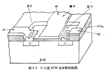
Figure 1-1N bubble MOS transistor structure diagram
As can be seen from the figure, from the metal gate downward is the silicon dioxide insulating layer, and then the semiconductor silicon below, so that the MOS system is composed of three layers of metal, silicon dioxide and silicon. If the gate-source voltage is not applied to the metal gate, the sources are separated by two "back-to-back" diodes, even if the voltage VDG is applied between the source and the drain, no current will flow, but only a very small PN junction leakage Current. But when a sufficiently large forward gate-source voltage VDG is added to the gate, an electric field directed to the silicon surface will be generated under the gate. When the gate-source voltage is greater than the value voltage VT of the MOS tube, the electrons in the P-type silicon body are attracted to the surface under the action of the electric field, forming an N-type layer with the opposite conductivity type in the body, which is called N-channel. The source and drain two diffusion regions are connected. When a voltage VDG is applied between the source and the drain, the current flows from the drain region to the source region through the channel, as shown in Figure 1-2. When the gate-source voltage a continues to increase; the electrons attracted to the inversion layer also increase (that is, the conductive channel becomes thicker and the resistance decreases), and the drain-source current increases rapidly with the increase of as. On the contrary, if the gate-source voltage decreases, the electrons in the inversion layer decrease, the conductive channel becomes thinner, and the channel resistance increases, so the current flowing through the channel will decrease. When the gate-source voltage is less than the value voltage VT, the channel disappears and ID=0. When VDG is constant, the relationship curve of source current ID changing with VDG is shown in Figure 1-3, which is called transfer characteristic curve.
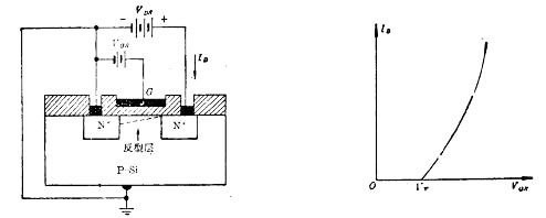
Figure 1-2 Schematic diagram of the working principle of the N-channel MO3 transistor Figure 1-3 Transfer characteristics of the N-channel enhancement type MO transistor
For the MOS transistor mentioned above, when the gate-source voltage VDG=0, there is no inversion channel in the Si surface layer under the gate oxide layer, and no current flows between the source and the drain. Only when the gate-source voltage VGS ≥ VT, the Si surface layer オ begins to form a strong inversion layer, and then a current starts to flow between the source and the drain. Devices that work in this way are called N-channel enhancement mode MOS devices.
If when the source voltage VGS=0, the original channel has been formed in the B surface layer under the gate oxide layer, as long as a small voltage is applied between, there will be current flowing between the source and the drain. Devices that work in this way are called N-channel depletion-mode devices. For example, when the P-type village bottom concentration is low and there are more positive charges in the gate oxide layer, it is often made into an N-channel depletion MOS transistor. Its transfer characteristic curve is represented by Figure 1-4.
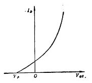
Figure 1-4 N-channel depletion type
MOS transistor transfer characteristic curve
It can be seen from the figure that when the gate-source voltage VGS increases from zero to the positive direction, the electrons attracted to the inversion layer increase, and the drain-source current increases with the increase of VGS. If the gate-source voltage VGS increases from zero to the negative direction, the electrons in the inversion layer are repelled by the electric field and decrease, and the drain-source current decreases accordingly; when the negative value of the gate-source voltage VGS reaches a certain value, the inversion When the layer disappears completely, the drain-source current drops to zero. We call the VGS at this time the channel pinch-off voltage of the device, which is represented by VT. It has the same meaning of the MOS transistor transfer characteristic curve as the valve voltage, so it is also represented by the threshold voltage VT. From the above analysis, it is known that the threshold voltage VT of the N-channel enhancement mode MOS transistor is > 0, and the threshold voltage VT of the N-channel depletion mode MOS transistor is < 0. Since the source and drain diffusion regions are formed in the same diffusion, from a structural point of view, there is no difference between the drain region and the source region. So, how are the source and drain determined: This is mainly determined by the bias conditions in the application. We define the diffusion region with the lowest potential in the N-channel MOS transistor as the source, and the higher potential as the drain. Under normal working conditions, the source and the bottom are connected together, so the drain is at a high potential relative to the bottom, that is, the PN junction between the drain region (N) and the bottom is reverse biased. In this way, when the MOS transistor is working normally, the diffusion area and the bottom of the village are mutually insulated.
2. P-channel suitable MOS transistor
If an N-type village bottom is used and two P-type source and drain diffusion regions are made on it, a P-channel MOS field effect transistor can be made. Figure 1-5 is a schematic diagram of the operating voltage bias of the P-channel enhancement mode MOS transistor. The source is grounded, the gate-source voltage VGS and the drain-source voltage VDS are both negative bias voltages, which are exactly the opposite of the voltage bias of the above-mentioned NMOS transistor.
Figure 1-6 shows the transfer characteristic curve of the P-channel enhancement mode MOS transistor. When the gate-source voltage |VGS| increases to |VT|, the inversion layer on the surface of the N-type substrate begins to form, and current starts to flow between the drain and source. When |VGS| continues to increase, the void in the inversion layer As the number of holes increases, the drain-source current increases accordingly. On the contrary, when |VGS| decreases, the drain-source current also decreases; when |VGS|<|VT|, the channel disappears, ID=0. P-channel MOS transistors manufactured by conventional processes can only manufacture enhancement mode MOS transistors.
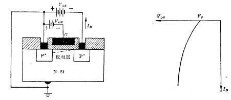
Figure 1-5 P-channel MOS transistor working principle schematic diagram Figure 1-6 P-channel enhancement mode MOS transistor transfer characteristic curve
Of course, P-channel MOS transistors should also be able to make depletion type, that is, when VGS=0, there is an original P-channel in the P-type silicon surface layer under the gate, and only add between the gate and source With a certain positive voltage, the original channel will disappear, making ID=0. The transfer characteristic curve of this tube is shown in Figure 1-7, where VT is a positive value.
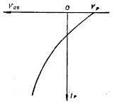
Figure 1-7 P-channel depletion channel MOS transistor transfer characteristic curve
From the above introduction, it is known that the voltage Vr of the P-channel enhancement mode MOS tube is negative, and the threshold voltage VT of the P-channel depletion mode MOS tube is a positive value.
Contact: Mr. Zou
contact number:0755-83888366-8022
mobile phone:18123972950
QQ:2880195519
Contact Address: 5C1, Block CD, Tianji Building, Tianan Digital City, Chegongmiao, Futian District, Shenzhen
Please search WeChat official account: "KIA Semiconductor" or scan the following picture to "Follow" official WeChat official account
Please "follow" the official WeChat account: provide MOS tube technical assistance


