Electronic Technology Forum
CMOS inverter working principle and detailed analysis of voltage transmission characteristics
The working principle of MOS inverter
The simplest inverter that can be integrated on a single substrate is an enhanced MOS load inverter. Its driving device and load device are both enhanced MOS, so the manufacturing process is relatively simple. The enhanced MOS load is often in the on state, and can be divided into a saturated area and a non-saturated area based on the difference in its working area, which are called saturated load inverters and unsaturated load inverters respectively. Although the manufacturing processes of E/D MOS and CMOS inverters are complicated, they have resulted in good circuit performance.
1-2-1 Learn the characteristics of load inverters
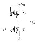
The load device of the saturated load inverter is an n-channel enhancement mode MOS working in the saturation region, which is usually realized by connecting the gate and the drain. The circuit diagram is shown in Figure 1-2-1. Since the gate and drain of the load device Ti are short-circuited and connected to the power supply VDD, the gate-source voltage of the load tube is equal to the drain-source voltage, that is, VDSL=VGSL, so the load tube always meets the condition VDSL>VGSL -VTL (where VTL is the turn-on voltage of the load tube), that is, it is impossible to form an inversion layer on the silicon surface near the drain terminal, so the load tube always works in the saturation zone. Compared with the resistive load inverter, the load device of the saturated load inverter is not a pure resistor, but a non-linear resistor; and the load tube is changed from the original three-terminal element to the two-terminal element.

(1) Working principle
The load tube works in the saturation region, and the relationship between the current and the voltage of TL meets the current equation of the MOS tube in the saturation region, and the gate and drain of TL are short-circuited, so the following relationship is obtained:

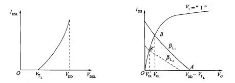
There is a square relationship between IDSL and VDSL. And because VDSL=VDD-Vo or Vo=VDD-VDSL, the formula (1-21) can be written as

The equation (1-2-2) is the load line equation of the saturated negative self-inverter, and Figure 1-2-2a is the load line of the saturated load inverter. Draw the load line and the output characteristic curve of the driving device together, and get Figure 1-2-2b.
When the input voltage of the CMOS inverter is low, the drive tube T1 is cut off, only a small reverse current flows, and the leakage current of the drive tube is approximately zero. The intersection of the load line and the curve when the drive tube is stopped is the off-state operating point. The voltage corresponding to point A is high level VoH, and the high level VoH is approximately equal to (VDD-VTL).

(2) Voltage transfer characteristics (voltage transfer characteristic curve)
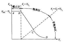
The static operating point only discusses the two states of on-state and off-state, that is, the output state when the input is high or low. If the input voltage value is between high level and low level, what is the state of the output? The voltage transmission characteristic curve gives the output voltage under various input voltage values. Therefore, the so-called voltage transmission characteristic curve refers to the relationship curve between the input level V1 and the output level Vo, as shown in Figure 1-2-3.
The voltage transmission characteristic curve can be deduced by the following methods:
(1) Write the current equation of the load device.
(2) When the input voltage value gradually rises from 0V to VDD, the drive device is in three different working states of cut-off region, saturated region and non-saturated region. Write the current equations of the drive device in each different working state.
(3) According to the circuit diagram in Figure 1-2-1, make the current of the drive device equal to the current of the load device. Since this equation is a function of input voltage and output voltage, it is the voltage transfer characteristic equation.
(4) According to the voltage transmission characteristic equation, obtain the output voltage data corresponding to the input voltage value rising from 0 volts to VDD, and draw the voltage transmission curve. It is naturally the easiest to draw the voltage transmission characteristic curve by computer simulation, but its calculation method and steps are consistent with the above.
The current equation of the load device of the saturated load inverter is given by the load line equation of (1-2-2).
The current equation of the driving device needs to be given after consideration in different areas:
(1) When 0<Vi<V1;, the driving device works in the cut-off region, and the current equation is:

(2) When VT1,<Vi<Vo+VT1, the driving device works in the saturation region, and the current equation is:

(3) When Vi>V0+VT1, the driving device works in the non-saturated region, and the current equation is:

In the formula, VT1 is the turn-on voltage of the drive tube T1. According to the above-mentioned steps [3], let the IDSL of the three regions = lDSL, and then obtain the voltage transfer relationship in three different working states:
(1) Cut-off area, 1/2βL (VDD-Vo-VTL) 2=0
After finishing: Vo=VDD-VTL=VOH (1-2-6)
That is the AB curve in Figure 1-2-3.
(2) Saturation zone, 1/2βL (VDD-Vo-VTL)=1/2βL[] (Vi-VTL) 2
After finishing:
in: 
That is the BC segment curve in Figure 1-2-3.
(3)Unsaturated zone,
After finishing:
This is the hyperbola of the CD segment in Figure 1-2-3.
In the voltage transmission characteristic curve of Fig. 1-2-3, the dividing line between the cut-off zone and the saturated zone is a straight line (l VI l=l VT1l), and the dividing line between the saturated zone and the unsaturated zone is a straight line (l VI l=l Vo +VTI l).

(3) Features of saturated load inverter
(1) Judging from the circuit diagram of a saturated load inverter (CMOS inverter), it uses a single power supply, with a simple structure and convenient design.
(2) Its output high level is a value where VDD-VTL is lower than the power supply voltage by a threshold voltage. Therefore, it is difficult to get the voltage transmission characteristic curve of the saturated load phase generator in Figure 1-2-3 to the expected high level, resulting in unnecessary voltage loss.
(3) Since the load tube always works in the saturation region, the power consumption of the inverter is large; in addition, when the output is close to the high level, the drain-source voltage of the load tube is small, and the gate-source voltage is also small, resulting in poor charging ability. Affect the working speed of the inverter.
(4) Its output low level and voltage transmission characteristics are all related to the ratio of the conduction factor of the drive tube and the load tube (βR=βI/βL). Bx is larger, its output low level is lower, and voltage transmission characteristics are better. Therefore, in the design of the saturated load inverter, the width-to-length ratio of the drive tube is always designed to be larger, and the width-to-length ratio of the load tube is designed to be smaller.
Contact: Mr. Zou
contact number:0755-83888366-8022
mobile phone:18123972950
QQ:2880195519
Contact Address: Block 5C, CD Block, Tianji Building, Tianan Digital City, Chegongmiao, Futian District, Shenzhen
Please search WeChat official account: "KIA Semiconductor" or scan the following picture to "Follow" official WeChat official account
Please "follow" the official WeChat account: provide MOS tube technical assistance


