Electronic Technology Forum
The most basic foundation of MOS tube integrated circuit-(inverter) analysis
The most basic unit of MOS-IC-inverter
The most basic MOS tube integrated circuit is a gate circuit that completes the logic "not" function, and it is the most basic unit of a digital circuit.
Because its output and input signal polarity is opposite, it is called "inverter".
The inverter consists of a load device and a drive device. The MOS inverter is shown in Figure 1-1-1. In practical applications, the load device can use resistors, p-channel enhancement mode MOS tubes, n-channel enhancement mode MOS tubes, and n-channel depletion mode MOS tubes. The driving device generally uses an enhanced MOS tube. This is because the gate and drain of the enhanced MOS tube are of the same polarity, which facilitates direct coupling between stages in the circuit. In addition, when the drive tube is turned on, it generally works in the non-saturated region of the transistor, and a small on-resistance in the non-saturated region can obtain a lower output low level.

(A) Resistive load (b) Enhanced load (c) Depletion load
Figure 1-1-1MOS inverter
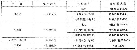
The load device of the inverter uses a MOS tube to replace the diffusion resistance, which can greatly reduce the area occupied by the load device in the integrated circuit chip; another advantage is that when the load MOS tube is used in the off state, the inverter can be reduced Power consumption. If the load MOS tube is controlled by the clock, the power consumption becomes a function of the clock duty cycle. There are many types of MOS load devices, which can be enhanced or depleted; they can work in saturated or unsaturated regions. Load devices and drive devices use various combinations of different types to form different types of inverters, as shown in Table 1-1-1.
Among the various types of inverters in the table, PMOS is a form adopted in the early days, but the conductive carriers of PMOS are holes, and their mobility is one-third to one-half that of electrons. With the maturity of NMOS technology, PMOS has been gradually replaced by NMOS. The enhanced/depleted MOS inverter (E/D MOS) has the advantages of high integration and fast switching speed, although it requires the manufacture of enhanced and depleted devices with two different threshold voltages on the same chip. After the ion implantation technology, the alarm voltage can be adjusted at will in the manufacturing process, so the N-channel E/D MOS circuit has become the main form used in the MOS large-scale integrated circuit. As for the advantages of CMOS inverters are low power consumption, high speed and strong anti-interference ability. It is the most superior one among the inverters listed in Table 1-1-1. Most of the current medium and large-scale MOS transistor integrated circuits Adopt CMOS form. Especially because of the micro power consumption advantage of CMOS, it is widely used in cosmic space technology, portable electronic computers and communication machines, electronic clocks and so on. Since this complementary circuit requires the manufacture of two different channel MOS transistors on a wafer substrate, the use of wells and the requirements for electrical isolation affect the integration level. However, with the current development of sub-micron process technology, CMOS circuits It has an absolute advantage in very large scale integrated circuits.

Table 1-1-1 The main types of MOS inverters
The above different MOS inverters can all be manufactured on a silicon substrate through different integrated process technologies. However, different inverter types, device operating modes, substrate materials and layout design details all determine and affect the parameters of the inverter: distributed capacitance, speed, power consumption, output swing, and so on.
This chapter first introduces different types of inverters, describing their output characteristics, static conversion characteristics, dynamic characteristics, and layout design. As for the use of p-channel or n-channel as a driving device, the basic characteristics are the same, but the polarity and certain parameters (such as mobility) are different. We use n-channel as the representative circuit for analysis. On the basis of the inverter, the basic gate and transmission gate of the circuit are introduced, and then various structures and operating modes of the flip-flop are introduced.

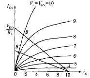
Figure 1-1-2 Characteristic curve and operating point of resistive load inverter
The resistance inverter of Figure 1-1-1a is composed of MOS tube (as a driving device) and diffusion resistor (as a load device). The input device is an enhanced N-channel MOS transistor T1. The current-voltage characteristic curves of T1 under different input voltages (ie, gate-source voltage Vcs) are shown in Figure 1-1-2. The current Ios flowing through the T1 tube is limited by the power supply voltage Vam and the load resistance RL. As can be seen from the line in Figure 1-1-1a, it satisfies the following relationship:

The above equation is also called the load line equation of the inverter circuit.
Since the current IDS flowing through the T1 tube is the same as the current flowing through the load resistance R, and the drain-source voltage VDs of the T1 tube is equal to the output voltage Vo, it can be on the current-voltage characteristic curve of the T1 tube, according to (1-1 -1) The straight line equation of the formula makes Vo∝IDS curve. The curve is a straight line, called the load line. The intersection of the negative section line and the x-axis (VDS axis) is (0, VDD, 0); the intersection of the load line and the y-axis (IDS axis) is (0, VDD/RL). The slope of the load line is △VDs/△IDS=-RL.
When the input voltage Vi is close to zero volts, the T1 tube is cut off, the reverse leakage current ID≈0, and the current-voltage curve of the T1 tube crosses the load I at point A. Point A is in the cut-off area of the T, tube. At this time, the output voltage is close to Va and the output is high. Point A is called the off-state operating point.
When the input voltage V.~Vam, T; the tube is fully turned on, T, the tube current and voltage curve intersects the load line at point B. Point B is at T; the unsaturated zone of the tube. At this time, the resistance at both ends of the drain and source of the T1 tube is very small (much lower than RL), and the power supply voltage VDD mostly falls on both ends of the load resistance RL, and the output is low. , Point B is called the open state operating point. The larger the load resistance RL, the smaller the slope of the load line and the lower the output low level, as shown at point B'in Figure 1-1-2.
In the case of a certain power supply voltage, the choice of load resistance RL is very important. In addition to the above-mentioned use of a large resistance to reduce the output low level, a large resistance is also required to reduce the power consumption of the circuit and increase the output logic swing. However, the diffusion resistor with large resistance occupies a large area in the chip, which is not conducive to the improvement of integration. Therefore, in the manufacture of MOS transistor integrated circuits, inverters all adopt the form of MOS transistors as load devices.
Contact: Mr. Zou
contact number:0755-83888366-8022
mobile phone:18123972950
QQ:2880195519
Contact Address: Block 5C, CD Block, Tianji Building, Tianan Digital City, Chegongmiao, Futian District, Shenzhen
Please search WeChat official account: "KIA Semiconductor" or scan the following picture to "Follow" official WeChat official account
Please "follow" the official WeChat account: provide MOS tube technical assistance


